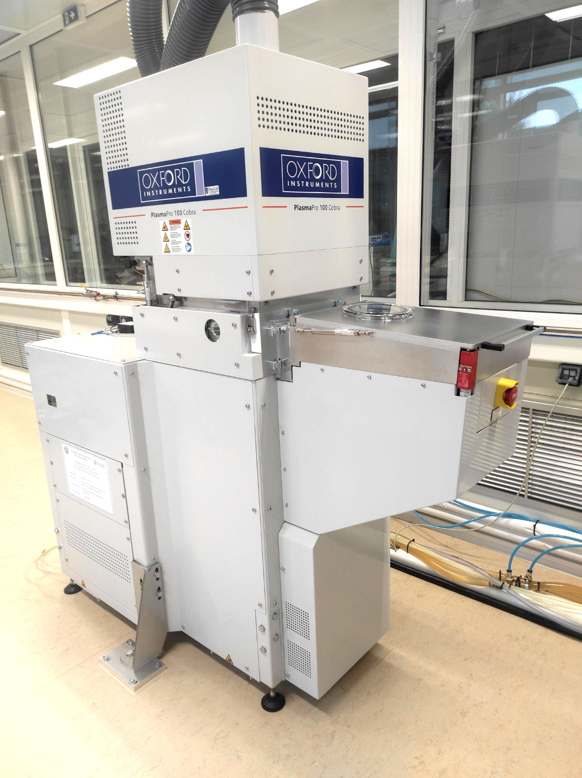
ALPES / Atomic Layer Plasma Etching System
PlasmaPro 100 Cobra
CONTACT PERSON:
Gogolides Evangelos
EMAIL:
e.gogolides@inn.demokritos.gr
PlasmaPro 100 Cobra
CONTACT PERSON:
Gogolides Evangelos
EMAIL:
e.gogolides@inn.demokritos.gr
Atomic Layer Etching (ALE) is an advanced etch technique that allows for excellent depth control on shallow features. As device feature size reduces further and further ALE is required to achieve the accuracy required for peak performance. High fidelity pattern transfer (etching) is essential for the fabrication of todays advanced microelectronics devices. As features shrink to sub-10 nm levels, and novel devices make use of ultra-thin 2D materials, there is a n increasing need for atomic-scale fidelity.
Applications
Dry etching of metals: Al, Cr, Si and polysilicon, Cu, adhesion metals such as Ti, Cr and Barrier metals such as Ni, Co, Ru. Noble metals such as Au, Pt, Pd, Ag.
Dry etching of oxides: SiO2, ZnO, TiO2, SnO, Indium Tin Oxide (ITO), CrO, NiO, Al2O3 (ALD deposited γ-Al2O3), HfO2, ZrO2, Y2O3, Ta2O5, WO3, MoO3, and Silicon Carbide (SiC).
Dry etching of Nitrides, Sulfides and other Compounds: Si3N4, TaN, TiN, AlN, HfN, GaN, AlGaN, MoS2, WS2, MoTe2, MoSe2.
Polymer film and polymer plate etching, as well as etching of organic materials.
Type
Mode capabilities: Inductively Coupled Plasma (ICP), Reactive Ion Etching (RIE) and Atomic Layer Etching (ALE).Coil Frequency (ICP)
13.56 MHz
Coil Power (ICP)
0 – 3000 W
Electrode Frequency (CCP)
13.56 MHz (HF) and 350 – 460 kHz (LF)
Electrode Power (CCP)
0 – 600 W
Electrode temperature
-30 – 400 οC
Pressure
1 – 100 mTorr
Gases
Cl2, BCl3, CH4, H2, O2, Ar, CF4, C4F8, SF6 and He
Samples Dimmensions
A wide range of wafer sizes can be processed, from small wafer pieces (1x1 cm2) up to 200 mm (8”) diameter