ABOUT
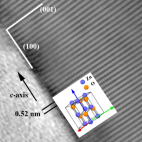
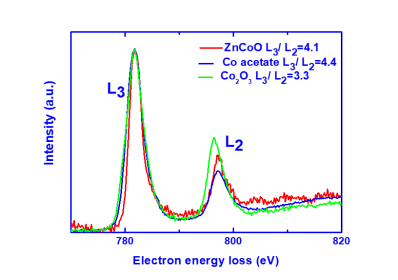
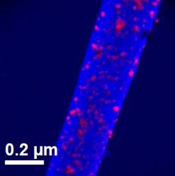
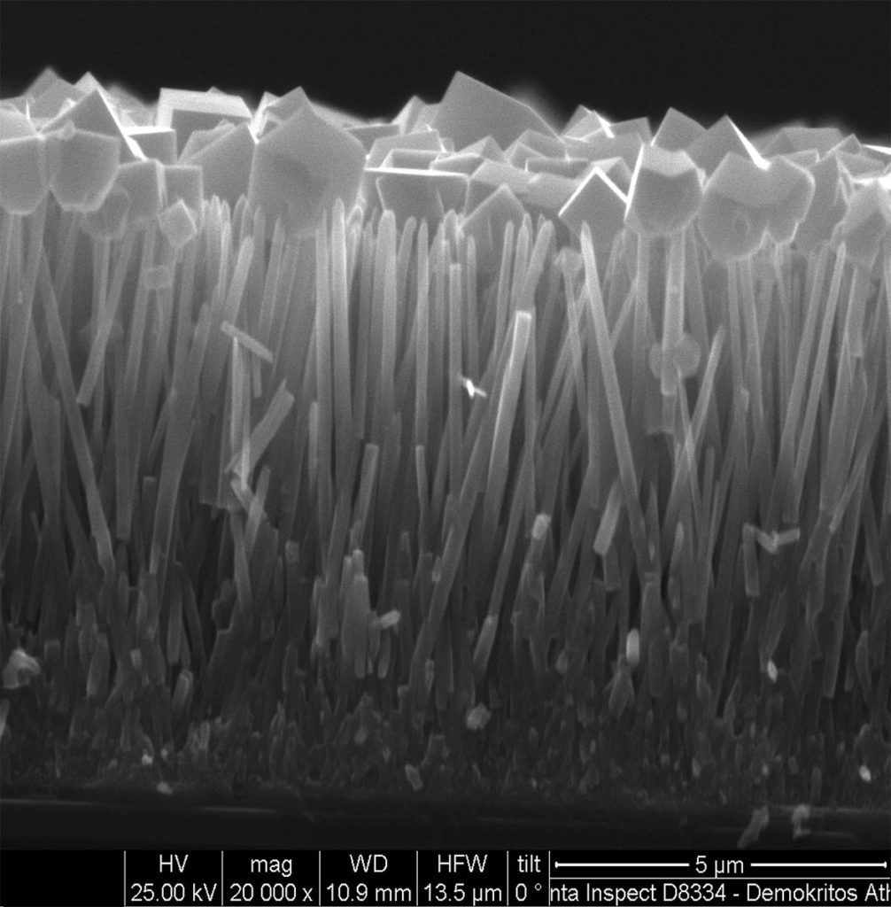
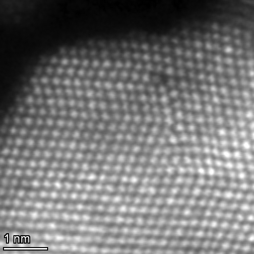
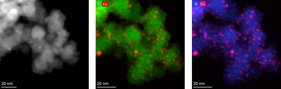
The Electron Microscopy Laboratory was established in 1987 with the acquisition of the first scanning electron microscope and under its current name Electron Microscopy and Nanomaterials Lab (EMNL) has been operating since 2014. The EMNL group focuses on the use of electron microscopy techniques in nanotechnology and materials science. In particular our research concerns the study of materials/nanostructures from the μm- down to the atom- scale, utilizing scanning and transmission electron microscopy, in order to investigate their key-nanoscale features and understand the correlation of these features to their macroscopic properties. This knowledge enables the optimization of growth/synthesis conditions as well as the design of new materials/nanostructures with improved and/or tailor-made properties.
Our main activities are:
• the study of microstructure by electron microscopy techniques of various advanced materials and functional nanostructures in order to optimize their growth and tailor their properties
• the growth and study of nanomaterials with applications in optoelectronics and energy
• Provision of research services to industrial partners
• Provision of education and training to undergraduate and graduate students in electron microscopy