ABOUT
The Epitaxy and Surface Science Lab (ESSL) started its operation as a Molecular Beam Laboratory (MBE) in year 2000 and has 25 years history of research on materials and devices for advanced CMOS and post CMOS nanoelectronics. Headed by Dr. A. Dimoulas, the lab raised around 10 million Euros from EU and national competitive projects, which allowed building new infrastructure worth of 3 million Euro and supporting a team of 9-10 members on average consisting of a senior scientist (Dr. A. Dimoulas), postdoctoral research associates and PhD students.
The research team has established:
- scientific excellence receiving two ERC grants (Advanced and Proof of Concept), as well as Marie Curie, FET, EIC and HFRI grants. Dr. Dimoulas has also received a Chair of Excellence appointment at CEA and the U. Grenoble Alpes for the development of MBE growth of 2D Materials and,
- leadership in European research by coordinating a number of large Industrial leadership (FP5-7 ICT, HE CL4) and Scientific Excellence (FET and EIC) European projects. Dr. Dimoulas is currently the director of a Romanian research team at NIMP, Bucharest in the framework of the Romanian recovery and resilience plan.
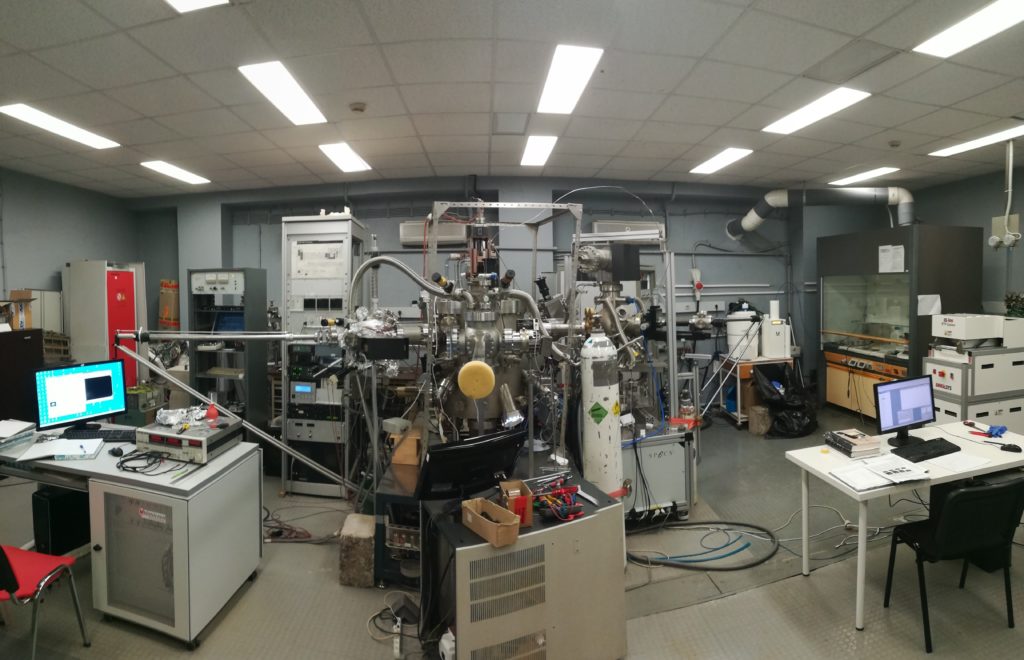
The last fifteen years, the lab has become a unique facility in Greece for Surface Science encompassing a number of surface analytic techniques such as Scanning Tunneling Microscope (STM), Reflection High-Energy Electron Diffraction (RHEED), X-ray and Ultraviolet Photoelectron Spectroscopy (XPS/UPS) and Angle-Resolved Photoelectron Spectroscopy (ARPES), all integrated with the MBE chamber for in-situ characterization of the grown thin films. ARPES is the only such technique available in Greece and among the few existing in European labs and around the work (except from the large-scale synchrotron facilities), which enables the imaging of the electronic band structure of crystalline solids. The lab is complemented by (a) a low T (5-320K) Kerr Microscopy and Magnetometry, (b) a CVD system equipped with a 4-inch cold wall chamber for the growth of graphene and for rapid thermal processing, (c) an electrical measurements facility consisting of a semiconductor device analyzer (Keysight B1500) equipped with a random waveform generation and fast measurement unit, a ferroelectric thin film tester, current source, nanovoltmeter and lock-in amplifier for Ηall-effect measurements, an LCR bridge for capacitance measurements and a micromanipulator stage for electrical evaluation of devices in the range 4-475K, (d) a chemical hood for simple device processing, (e) a high-performance workstation for first principles calculations based on Density Functional Theory (DFT), (f) a high precision, fully motorized thin film transfer stage for 2D materials transfer and precision positioning.
In brief, the main achievements of the lab and its contribution to the worldwide research are:
- Development of Germanium MOS technology for the scaling of advanced CMOS (widely cited).
- First investigation in Europe of elemental 2D materials silicene and germanene (“cousins” of graphene), as well as the 2D graphitic AlN material (widely cited)
- Development of the MBE growth of 2D transition metal dichalcogenide materials, with topological and ferromagnetic properties with an impact in energy efficient spintronic logic and memory.
- Development of Hafnia-based ferroelectric tunnel junction memristors functioning as electronic synapses for next generation, AI-powered chips.
Evaluation by external experts:
The ESSL team has been very positively evaluated by external experts, during the INN evaluation process.
Among others, the experts wrote: “…This group should make a role model for the structure, mentality and quality of research for the sort of groups INN should aim to build.”
and,
“This group has the closest structure one typically finds in highly performing research groups abroad, i.e. one single PI with several postdocs and PhD students and an outstanding track record of funding, research output and state-of-the-art facilities. The group has demonstrated capacity and potential to evolve and change fields systematically, building upon previous expertise and knowledge but always expanding into new directions. This is a very healthy approach for high-quality research and the group has very strong potential for growth in the future.”
To read the whole report, please follow this link.