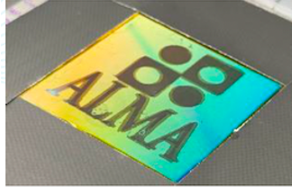
Adaptable Large area Meta-surfaces for customised Αpplications
https://nkehagias.wixsite.com/alma-project-gr
ACRONYM:
ALMA
LEADER:
Nikos Kehagias
START DATE:
01/01/2023
LATE DATE:
31/12/2025
FUNDING SOURCE:
HFRI
https://nkehagias.wixsite.com/alma-project-gr
ACRONYM:
ALMA
LEADER:
Nikos Kehagias
START DATE:
01/01/2023
LATE DATE:
31/12/2025
FUNDING SOURCE:
HFRI
Nanoenabled devices and components emerging from precise control of the surface structuring provides enhanced benefits directly related to efficiency, cost effectiveness, reliability and low energy consumption. Key innovations in alternative imprint-based techniques have resulted in an entirely new generation of devices and products with affordable cost providing added value functionalities in a disperse range of materials. Nanophotonic components and devices control and manipulate light by altering its phase, amplitude and polarization states in a desired manner. Wavefront shaping through the control of phase, amplitude has opened a new era of flat optics applications in the areas of integrated optics, holography, flat displays, energy harvesting and mid-infrared photonics. In this instance artificial media, namely metasurfaces, with sub-wavelength thickness consisting of single (or few) layered alternating materials, in the wave propagating direction, enable new functionalities and phenomena which are not found in nature.
The objective of ALMA project is to develop a flexible technology for adaptable large area functional metasurfaces applications based on smart (optical) designing, alternative nanofabrication process and post printing technologies. The proposed technology will enable the production of large area optical templates (surfaces), which after a post printing process, will provide tailored functionalities for applications in areas such as security printing, optical and energy harvesting systems.