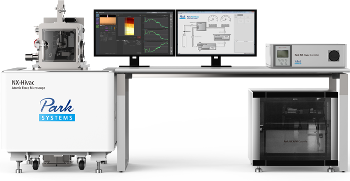
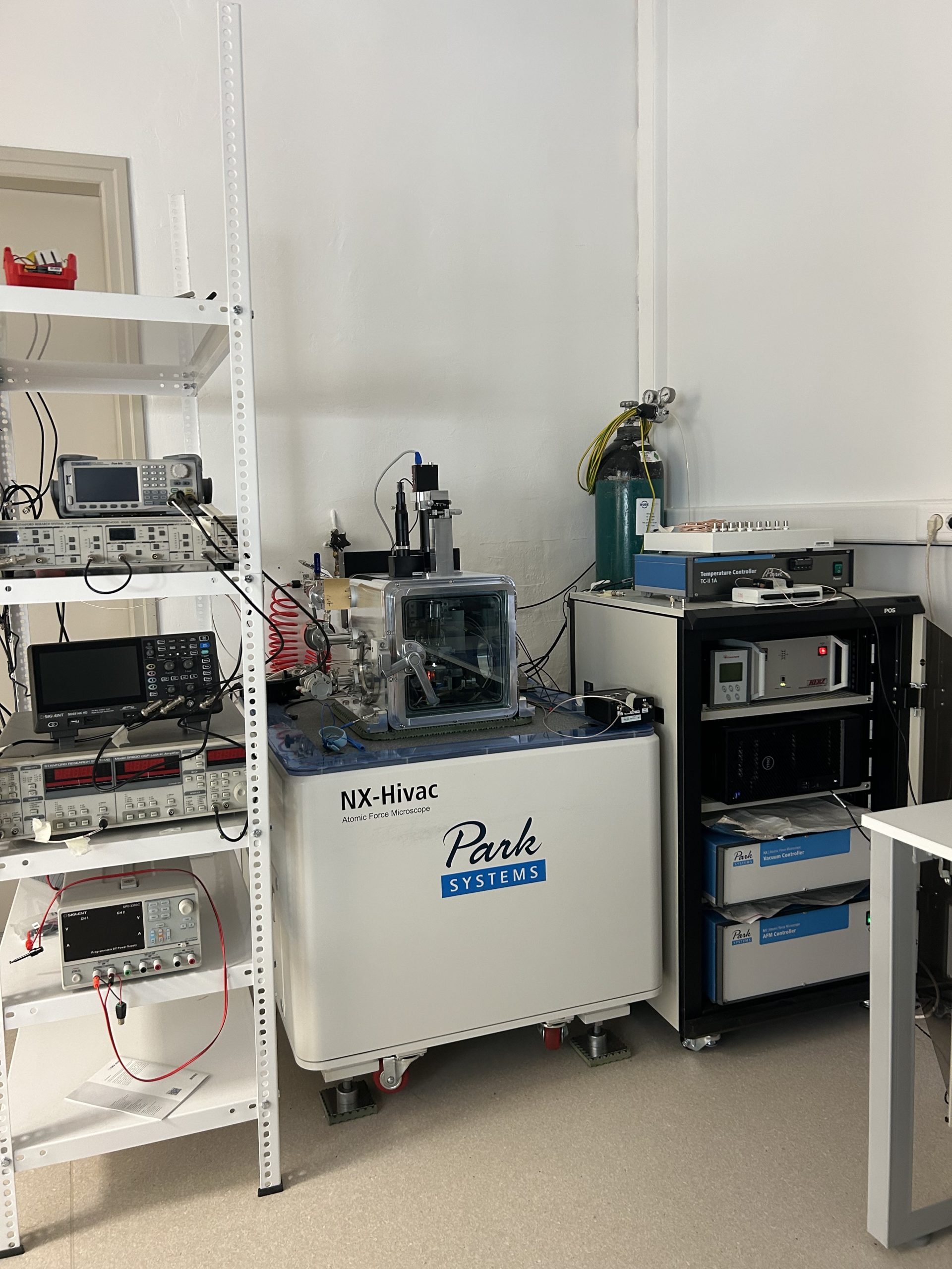
High-vacuum scanning probe microscope (SPM)
Our high vacuum scanning probe microscope (SPM) is ideal to explore mechanical, electrical, thermal and thermoelectric properties of low-dimensional materials. Operating in a high vacuum environment, it delivers enhanced accuracy and repeatability, minimizing tip and sample damage. We focus on the following SPM modes:
- Piezoelectric force microscopy (PFM) to probe electromechanical material properties on the nanometer scale in addition to the sample topography.
- Conductive AFM (C-AFM) to simultaneously measure the topography and conductivity of a sample by scanning the surface with a conductive material coated tip as a nanoscale electrical probe at an applied DC bias.
- Kelvin probe force microscopy (KPFM), an electrostatic force microscopy (EFM) technique to study the electrical surface properties of various conductive or semiconductive samples. KPFM provides quantitative results of the local surface potential distribution or the work function of the sample.
- Scanning Thermal Microscopy (SThM)/Scanning Thermal Gate Microscopy (STGM) to explore nanoscale thermal phenomena for applications in nanoelectronics and energy conversion. These include conventional and unconventional nanoscale devices, neuromorphic devices and thermoelectricity.
Images