Eaton NV-3204
CONTACT PERSON:
Dr. Vassilis Vamvakas
EMAIL:
v.vamvakas@inn.demokritos.gr
CONTACT PERSON:
Dr. Vassilis Vamvakas
EMAIL:
v.vamvakas@inn.demokritos.gr
Applications
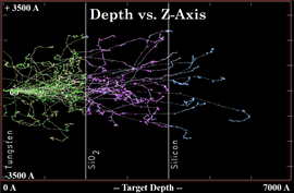
Ion implantation (II) allows for introducing in a controllable way energetic atoms or molecules into a solid to alter its physicochemical properties. Selective implantation can be achieved by means of a patterned masking material (e.g., SiO2, Si3N4, photoresists) formed onto the surface of the target material. In addition to Si, Ge and compound semiconductor doping for the fabrication of a wide range of devices (e.g., diodes, MOSFETs, Bipolar transistors, MESFETs), II is also employed for other applications including: Modification of insulating layers, Fabrication of Si nanocrystals, Modification of polymers and nano-composite materials, etc.
Technical Specifications
Medium Current / Medium Energy Ion Implanter
20 – 200 keV (selectable in 1 keV increments)
Up to 500μΑ
B, BF2, P, As, N, Si, Ar
Better than 0.75% / 0.5%
125 AMU at standard extraction voltages, M/ΔΜ > 100/1
Adjustable 0 to 15 degs
From 4” wafer down to 1 cm x 1 cm square samples
Clean-room ISO 6 (Class 1000)