Low power sensors on silicon and flexible substrates
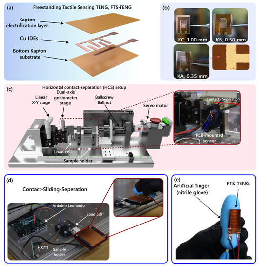
3.a Flexible tactile sensor for material and texture identification based on the triboelectric effect
We have developed a flexible triboelectric tactile sensor based on the freestanding single-electrode triboelectric nanogenerator principle, enabling concurrent material and texture detection within a single device. Our approach introduces a hybrid operational regime that merges the benefits of both contact-separation and surface sliding modes into one contact-sliding-separation motion. This allows a realistic surface representation using an artificial finger, extracting material information from contact-separation events and texture details from the sliding motion. For the identification study, common materials such as wood, paper, copper, and glass were used, along with textured variants of these materials featuring microscopic surface features. Simultaneous material and texture classification was performed with a single 1D convolutional neural network, achieving an average recognition accuracy of 98.4% across all surfaces.
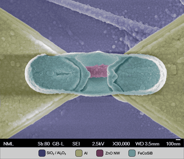
3.b Magnetic strain-gated transistors (M-SGTs)
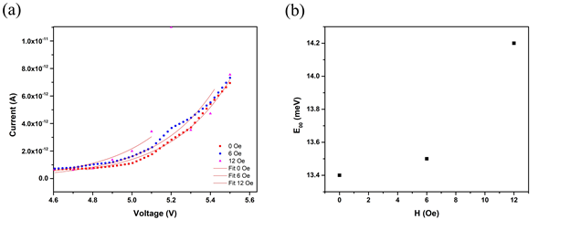
We have developed novel magnetic strain-gated transistors (M-SGTs) based on suspended ZnO nanowires. In recent years, there has been growing interest in sensors capable of detecting low-intensity magnetic fields at low frequencies. Sensors built from composite magnetoelectric materials offer advantages such as high sensitivity and a broad operating range from DC to hundreds of kHz at room temperature. These composites combine magnetostrictive and piezoelectric components, and despite ongoing efforts toward device miniaturization, nanoscale implementations remain relatively underexplored. The fabrication of M-SGTs was demonstrated for the first time using ZnO nanowires together with previously developed magnetostrictive FeCoSiB thin films. Experimental results verify the ability to control and tune current transport through a single ZnO nanowire with an external magnetic field, advancing the realization of magnetoelectric devices at the nanoscale. (A. Bardakas, Experimental and theoretical study of magnetic strain-gated transistors, based on semiconducting nanowires, PhD, Univ. of Patras, 2023)
3.c Photodetectors
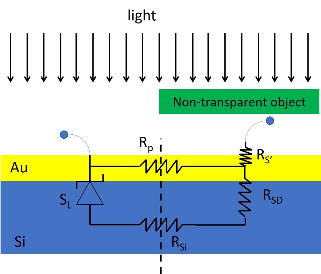
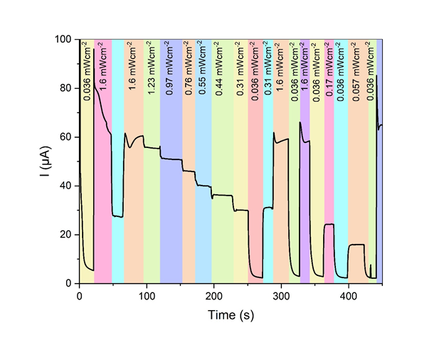
Photodetectors are an essential device in the field of optoelectronics. More specifically, the detection of the intensity of light has become very important in everyday applications such as smart building shading, lighting, automatic car headlights etc. In this category of applications cost is a very significant driving force. Moreover, with the advent of the Internet of Things (IoT), sensor systems inevitably move in the direction of self-powering. This stems from the impractical nature of battery replacement in networks with large numbers of sensor nodes. So, ideally, a photodetector designed for such everyday applications should be extremely cost effective, integrable with Si-based electronics and self-powered or, at the very least, not energy consuming. Our work focuses on the development of photodetectors using Schottky diodes and the “shadow effect”. Through these concepts efficient and cost-effective photodetectors can be created. Moreover, these photodetectors harvest enough energy from the incident light to be completely energetically autonomous.
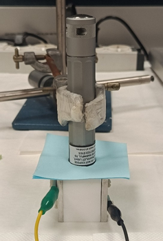
Another example of photodetectors developed within our laboratory is a novel-type of UV photodetector based on ZnO nanowires, namely an “electrolytic” photodetector. UV detection is crucial in several applications ranging from medical to communications. By using nanostructured ZnO, namely nanowires, a material with a band gap at the appropriate energy for UV absorption, combined with an electrolytic cell-type architecture we can create very low power (range of a few μW) detectors of high selectivity, enhanced sensitivity and relatively high detection speeds.
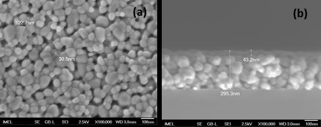
3.d Chemical sensors
Semiconducting metal-oxide chemical sensors have been of great interest for the last 30 years and extensive research has been made to better determine and optimize their sensing characteristics. Among these materials zinc oxide (ZnO) has been demonstrated to show great stability, low cost, relative ease of fabrication and sensitivity to several common gases, such as CO, H2, NO2, NH3, O2, ethanol, etc. Over the last decade there is an increased interest in growing ZnO nanostructures and/or nanostructured films using solution-based hydrothermal techniques, which have low cost, can be applied in hard as well as flexible substrates, are environmentally friendly and can be easily tuned to control the morphology and properties of the grown ZnO films. Moreover, it has been demonstrated that the electrical properties of the nanostructured films, which are n-type in principle, can be tuned by incorporating certain dopant atoms, such as lithium, during the growth process. Our work focuses on the design and development on Metal Oxide and ZnO based sensors aiming for food quality, safety and security and environmental monitoring.