Materials and technologies for sensing and energy harvesting
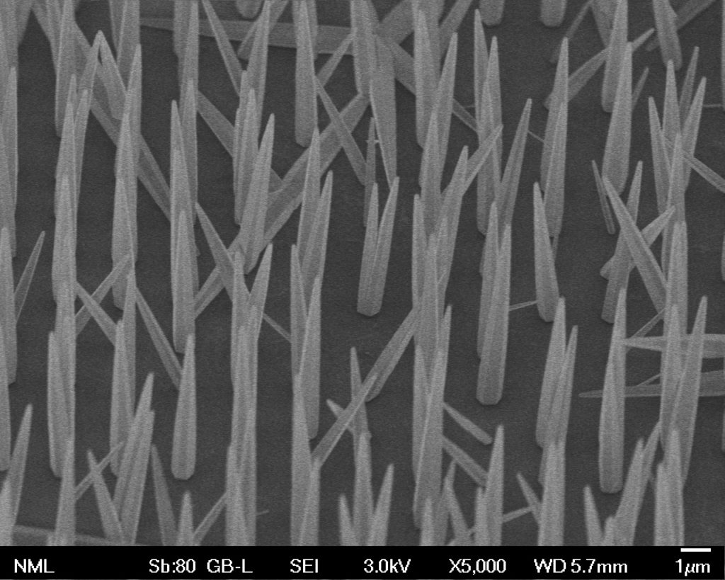
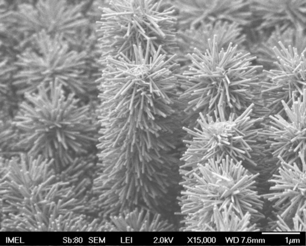
1.a Hydrothermal growth of ZnO nanostructures
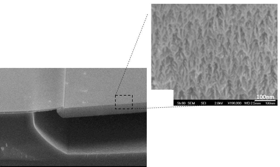
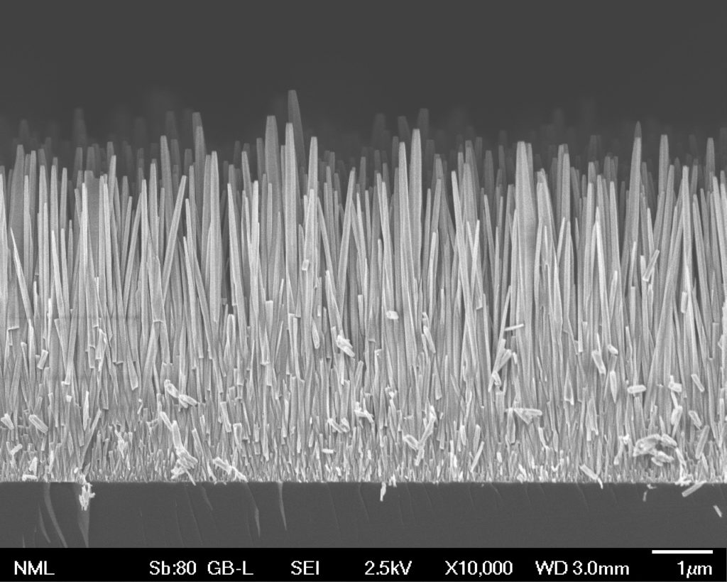
Zinc oxide (ZnO), a wide and direct band gap (3.37 eV) semiconductor possessing high exciton binding energy of 60 meV, has been recognized as one of the promising nanomaterials in a broad range of high-technology applications in optoelectronics, photovoltaics, energy harvesting and sensors. Over the last decade extensive effort has been directed toward the growth of well-controlled crystalline ZnO nanowires synthesized by low temperature, low cost and large area hydrothermal methods. Our work focuses on the growth on various ZnO nanostructures, including nanowires, nanowire arrays, 3D networks, etc. for sensing and energy harvesting applications.
1.b Hydrothermal techniques for synthesis of Carbon Quantum Dots
Carbon-based Quantum Dots (CQDs) are the newest member in the carbon nanoparticle family. Owing to their chemical inertness, low toxicity and facile functionalization of their surface chemistry, combined with unique optical properties such as photoluminescence and resistance to photobleaching, they have attracted significant interest as candidates for various applications ranging from OLEDs to chemical sensors, bioimaging and photocatalysis. Despite their extensive research, to date, their optical properties and the underlying mechanisms have not been yet fully understood, partially due to the various synthetic routes available, which lead to different types of CQDs. Our work focuses on the synthesis of CQDs with controlled properties as well as the study of their chemical properties for chemical sensing.


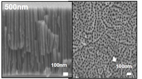
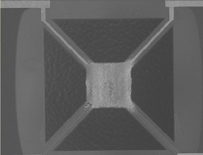
1.c Electrochemical porous materials on Si
Electrochemical porous materials have very interesting properties that are studied by the field of nanoscience and nanotechnology. They are used in novel devices for electronics, photonics and sensors, and find applications in different fields, including the information and communication technologies, health, medicine, environment and different other fields of human activity. More specifically, the focus of our group is in porous anodic alumina and porous Si. Porous anodic alumina is a self-organized porous material with pore arrangement in hexagonal symmetry. Our work focuses on the creation of this material for application as the dielectric material in MOS memory devices, WORM memory devices and MIM capacitors as well as a template for the formation of nanostructured composite materials. On the other hand, porous Si is a material composed of a skeleton of interconnected Si nanowires and nanodots. Due to its low dimensionality this material exhibits very different properties from those of bulk Si, including a much lower electrical and thermal conductivity, higher Seebeck coefficient and much higher surface area. Our work focuses on the local creation of porous Si on Si substrates for radiofrequency shielding from the Si wafer, local thermal isolation for thermal sensors, microhotplates for chemical sensors and thermoelectrics, as well as on-chip energy storage.