Optical sensors and characterization of metasurfaces and integrated photonics
Spectroscopic characterization of metasurfaces and photonic integrated circuits
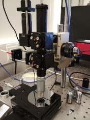
We use reflectance spectroscopy in a broad wavelength range (Vis-NIR) and a variation of optical reflection microscopy. The setup allows for simultaneous imaging and measurement of the reflectance, transmission, and photoluminescence spectrum from a region of a few square micrometers.
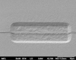
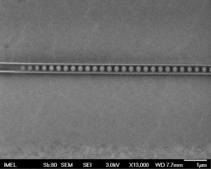
We designed and fabricated silicon nitride nanobeam cavities towards simultaneous localization of light and elastic waves in the same volume.
More information:
L. Athanasekos, A. Christofi, G. Gantzounis, E. Bolomyti, G. Papageorgiou, M.-C. Skoulikidou, I. Raptis, N. Papanikolaou, Microel. Eng. Volume 159, June 2016, Pages 42–45
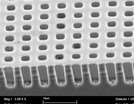
Fabrication of metal covered hole arrays in Si as efficient IR absorbers-emitters. We have studied hole arrays in Si with few micron diameters, covered with a thin Al layer. The fabricated structures were characterized with FTIR and the goal was to develop narrow band infrared emitters operating around 3-5 micron wavelengths. Typical structure is shown in the figure.