Thin Film Transistors
Low-cost high gain MoS2 FETs from amorphous low mobility film precursors
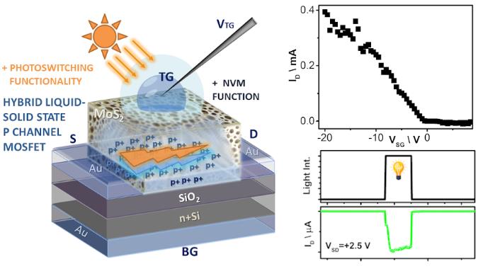
With the aggressive invasion of thin film transistors (TFTs) in the rapidly altering/disposable portable electronics, displays, smartphones and wearables market, cost reduction has evolved into a challenge as much as the improvement of their electrical properties. Therefore, it is not surprising that processes requiring expensive equipment and energy-intensive processes are abandoned in favor of Room Temperature (RT) approaches, liquid phase deposition and colloids. Despite being cheaper, the latter suffer from controllability, performance and large contact resistance issues, deteriorating the quality of the final product. To meet the trends while not compromising the performance, we fabricate a MoS2-based ionic liquid gated TFT with ON-current of 1.5x10⁴ A for holes and a field effect mobility of 64.3 cm2V-1s-1 at RT in a hybrid liquid-solid state 3D topology, utilizing low energy expenditure impurity tolerant processes. The device addresses the weakness of unattainability of P-type conduction in MoS2, thereby extending its pertinence to PN diodes and complementary integration logic. In addition, photo-enabled switching and memory functionality is demonstrated and detailed material and electrical properties are investigated. The herein presented advanced architecture is, to our knowledge, the first low-cost high gain MoS2 metal-oxide-semiconductor field-effect transistor (MOSFET) based on amorphous low mobility film precursors that enables high-performance multifunctional stackable MOSFETs on any kind of processing-sensitive, plastic and/or flexible substrate.