FEG HR Scanning-Transmission Electron Microscope (FEG S-TEM)
Tool
Thermo Fisher Scientific Talos F200i S/TEM
Applications
Conventional & High Resolution Transmission and Scanning / Transmission Electron Microscopy, Energy Dispersive X-ray Spectroscopy (EDX)
Source
Field Emission Gun
Beam Voltage
200kV
Detection
16 Mpixel CETA CMOS camera
4kx4k STEM imaging
Triple Thermo-Fisher 3 detectors system bright field (BF), segmented annular dark field (DF1,DF2)
Fischione 3000 high angle annular dark field detector (HAADF)
EDX Bruker 6|T Flash 100 mm2 (light elements sensitivity down to Be)
Resolution
TEM point resolution: 0.25nm
TEM information limit: 0.12nm
STEM resolution: 0.16nm
Positioning
x,y movement: α tilt = ± 35o, β tilt = ± 30o
Other Capabilities
4 available S/TEM detectors: HAADF, DF4, DF2, BF
max solid angle for EDX: 1.3srad


Additional equipment:
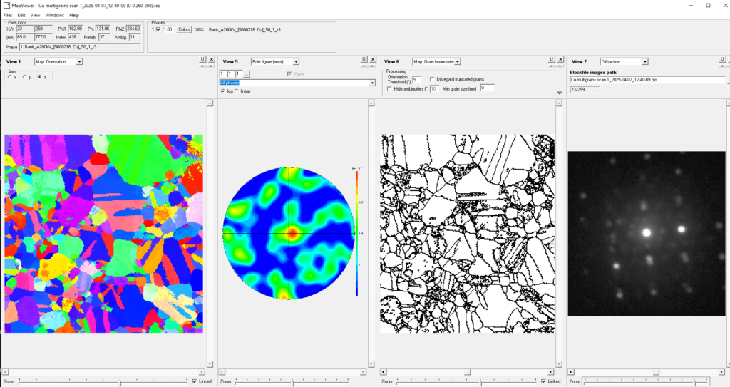
NanoMEGAS
Hardware: DigiSTAR
Software:
TEM Orientation Imaging (ASTAR): This is a technique similar to Electron Backscattered Diffraction (EBSD) in Scanning Electron Microscopy (SEM), but it provides crystallographic orientation and phase maps at a much higher resolution (down to 1-3 nm).
Strain Mapping: This allows for the analysis of strain fields in a material with high sensitivity. Electric Field Mapping: A more recent application, this technique uses 4D-STEM to study local electric fields and built-in potentials in functional materials.