Processing issues of ALD Al2O3 thin films on semiconductor substrates
(Contact person: V. Ioannou-Sougleridis)
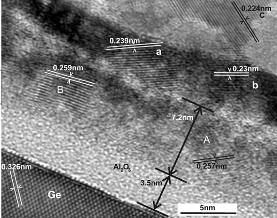
Initially, the aim of the activity was the study of the atomic layer deposited high-k materials and to explore the usability of such materials (HfO2, ZrO2 and Al2O3) in charge trapping non-volatile memory stacks. The main study was focused in the compatibility of high-k dielectrics as control oxides. This was accomplished by joint research activities with the Department of Chemistry of Helsinki University and the Department of Physics of Patras University. Thus, major parameters of the atomic layer deposited materials such as the type of the metallic precursors, the type of the oxidant, the deposition temperature and the post deposition annealing schemes were linked to the performance of the memory cells and especially to the retention characteristics. This research was a continuation of the previous activities in the non-volatile memory field of research utilizing silicon LE-IBS into a silicon nitride layer and subsequent wet oxidation, which provided good trapped charge retention properties. This activity fueled also a new one that of the study of the processing issues of ALD-Al2O3 on semiconductors substrates which investigates in what respect the standard photolithography influences the properties of the ALD-Al2O3 layers, as a result of wet processing in the various solutions employed. The activity utilizes MOS capacitors to study their electrical characteristics as well as structural studies. The new activity is conducted in collaboration with the Department of Physics of Patras University and up to now 4 students had completed their dissertation thesis.