Junctionless Si-nanowire FETs
(Contact person: P. Normand)
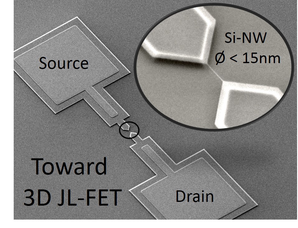
These activities started in 2014 with the motivation of providing a substantial added-value in the non-volatile memory field and Si-NW device technology. There were also intended to create a Si-NW technology platform in Greece for inciting and supporting research at the institute and national levels in digital electronics including the wide-ranging area of sensing electronics. Within the national project “NanoWireMemory”, a technology based on Junctionless (JL) FETs and ONO stacks has been set up for producing memory cells beyond the 22nm node. Devices with gate length (GL) and width (GW) ranging from 20nm to 1μm for both logic and memory applications have been successfully fabricated at the INN Nanotechnology & Microsystems Laboratory. JL Si-NW FETs of GL / GW down to 20nm / 40nm with state-of-the-art performance were demonstrated.
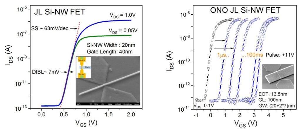
Further testing of ONO JL Si-NW FETs (13.5nm EOT) with a channel doping as high as 1.5x1019 cm-3 revealed excellent device features in terms of field-effect mobility (> 250 cm2/V.s), and subthreshold swing (~ 80 mV/dec) with no significant DIBL effect. Memory testing has shown encouraging write/erase and data retention characteristics. Interestingly, a dependence of the threshold voltage on GW smaller than 10mV/nm was detected. Additional experiments are under way to examine further this attractive feature as the high sensitivity of Vth on GW variation remains a critical issue in JL FET technology. Further research in that area include the development of GAA JL NW FETs and related memories.