Front-end processes for Ge MOS technology
(Contact person V. Ioannou-Sougleridis)
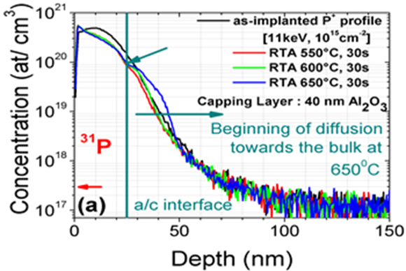
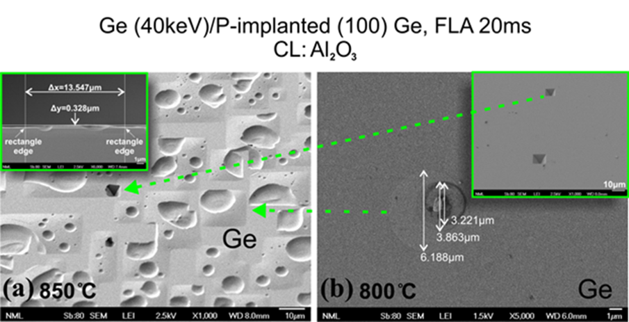
This research activity explores the possibility to replace silicon as channel material in CMOS technology by a higher mobility material. Such a replacement could relax the scaling constrains of MOSFET devices in logic applications. Ge possesses the higher hole bulk mobility among semiconductors materials and a higher than Si electron bulk mobility. This activity is conducted in collaboration with the Depts. of Physics of Patras and Thessaloniki Universities. The research objectives are twofold: a) the fabrication of a well passivated Ge-insulator interface and b) the fabrication of shallow and highly activated n+/p junctions through tight control of the fast diffusion of n-type dopants in Ge. The first objective is addressed by the formation of Ge MOS capacitors, utilizing mainly atomic layer deposited Al2O3. This approach revealed many unknown parameters of the Ge MOS technology which ultimately control the Ge-dielectric interface quality. These include the gate metal, that could act as interfacial oxide layer scavenging agent (Al), the reaction between the gate metal and the alumina layer (Pt), and the influence of the post metallization annealing. The second objective was accomplished using co-implants of nitrogen and phosphorus, followed by an annealing process. It noteworthily that Applied Materials Inc expressed interest in this approach and a collaboration was established in this activity. N and P co-implants in Ge results to a significant retardation of P fast in and out-diffusion. The best phosphorus activation value in our approach is 6x1019 cm-3, for rapid thermal annealing conditions of 600 oC for 30 min. Several type of annealing processes such as flash lamp annealing, rapid thermal and furnace annealing were explored, for process window optimization. In addition, extended defects, resulting from implantation damage and extreme thermal budget conditions were investigated.