Integration of III-V semiconductor compounds and devices with silicon
The integration of III–V semiconductor devices (e.g., LEDs, HEMTs) and systems (RF-MEMS) with silicon has received a great deal of attention in recent years. This technology offers the possibility to combine the optical and electronic functionality of III–V components with silicon technology. As an example, III-V photonic components could enable on-chip optical interconnects, thus increasing data transmission speed and lowering power consumption.
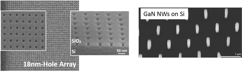
(1) SiO2 nanopatterning for selective-area growth of GaN nanowires on silicon - (Contact person: P. Normand)
Our activities in the field started in 2013. They were conducted within the "NanoWire" THALES national project coordinated by the University of Crete addressing the monolithic integration of GaN semiconductor compounds with Si. Our task was to fabricate nanopatterns into SiO2 films for the selective-area growth of vertical GaN NWs arrays on Si substrates. A large-scale SiO2 patterning process was developed based on e-beam lithography and subsequent reactive ion etching. Hole patterns with diameter ranging from 18 to 200nm and pitch in the 50nm to 10μm range have been successfully fabricated on 3-inch Si (111) wafers in square and hexagonal arrangements. Subsequent selective growth of GaN-NWs by plasma-assisted MBE was further demonstrated at IESL/FORTH.
Research in this area is currently underway with the support of Innovation-EL, the Greek Infrastructure Network for Nanotechnology, Advanced Materials and Micro/Nano electronics. Focus is on the selective-area growth of GaN and InN nanowires on III-V thin films formed onto Si substrates. A plasma-free process for the nanopatterning of SiO2 layers grown at low-temperatures has been developed and large-scale hole patterns with effective diameter as low as 30nm have been achieved in 2021. This research is conducted in collaboration with IESL/FORTH.
(2) Bonding of RF GaN chip modules on Si-wafer interposer for chip cooling (Contact person: P. Dimitrakis)
Heterogeneous and monolithic integration of III-V devices and RF MEMS with silicon are particularly appealing for technologies such as 5G wireless networks. They allow high-density packaging of components but led to serious heat dissipation concerns. Our work in this area started in 2019 within the “RADAR” project coordinated by IESL/FORTH. A critical task of the project is the integration of reconfigurable microwave power transceivers with silicon interposer for heat dissipation. Our involvement includes: (1) low-temperature ( < 200oC) eutectic bonding of GaN chip modules on Si using Sn-doped Al and Cu thin films and (2) dry etching-based fabrication of through-silicon-vias (TSVs). Very-dense TSVs have been demonstrated and optimized in terms of dimension accuracy and density, and wafer stress.