Si Sensors and Micro- Electro- Mechanical Systems (MEMS)
The group possesses great experience in the design and fabrication of Si based micromechanical and electronic devices. It is a member of the Nanoelectronics, Photonics and Microsystems Program of the Inst. of Nanoscience and Nanotechnology and is an integral part in the day-to day operations of the 300 sq. meter, fully equipped for Si processing clean room maintained by the that Program.
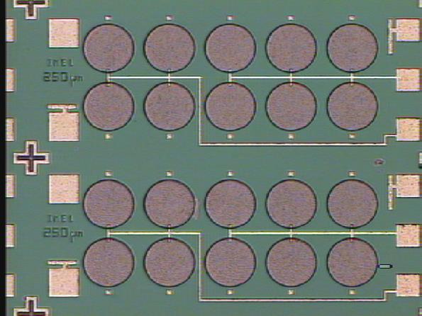
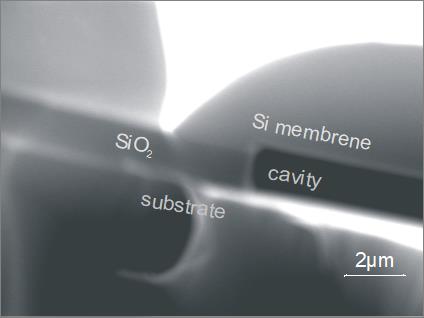
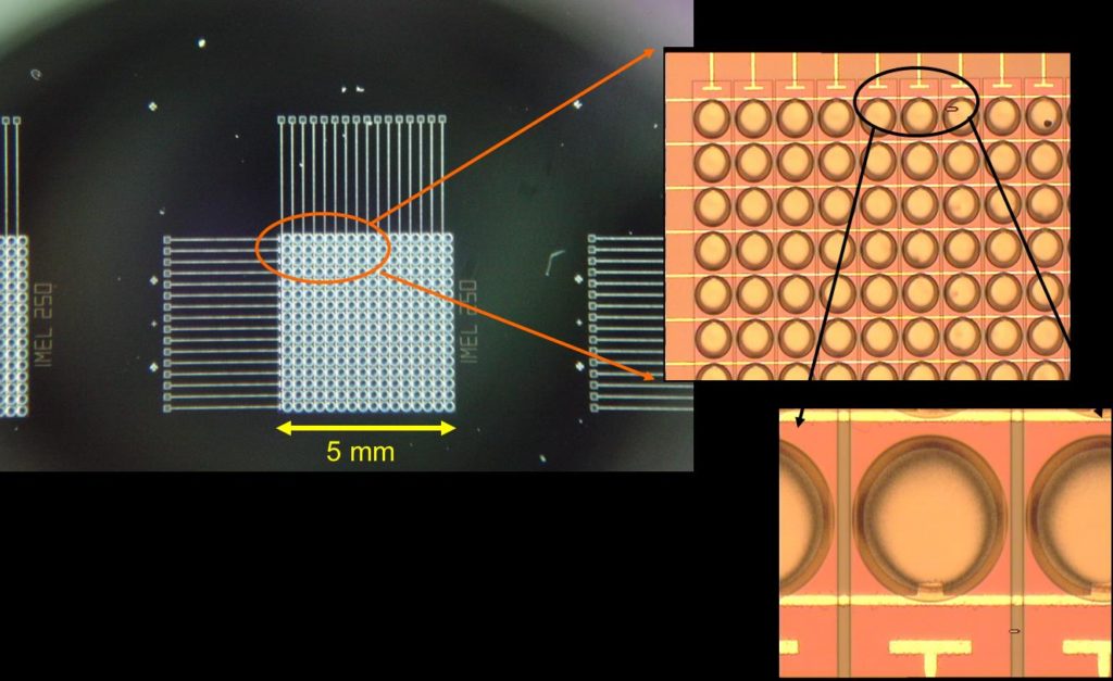
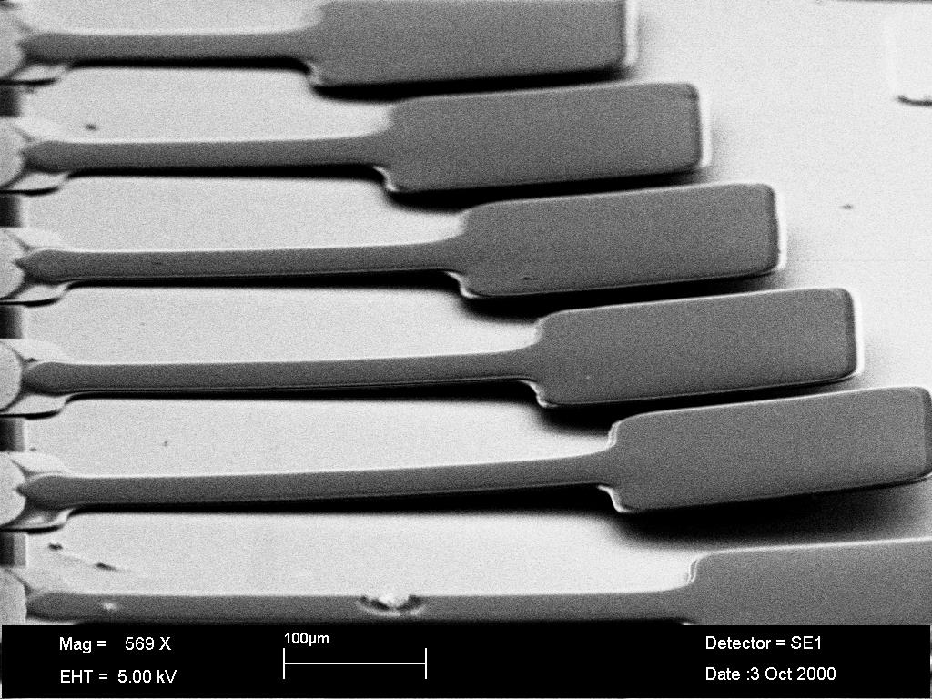
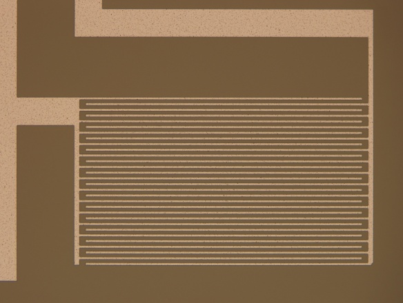
Next are showcased some examples of devices that have come out of our Clean Room. These have been fabricated using a number of Si microelectronic and micromachining techniques including Si Fusion Bonding and Si anisotropic etching.