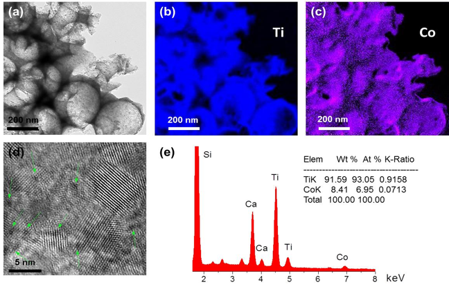
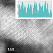
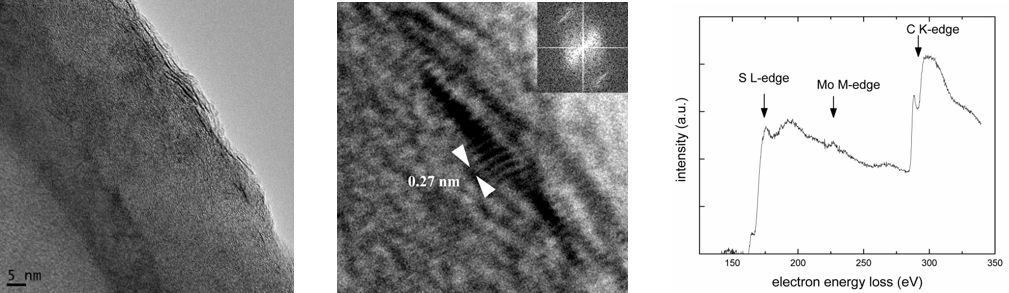
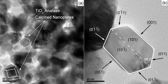
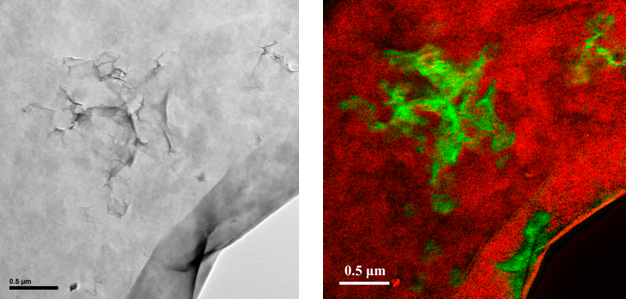
TEM characterization of materials and nanostructures
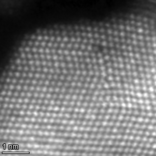
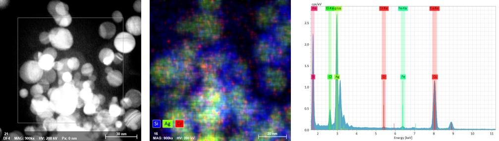
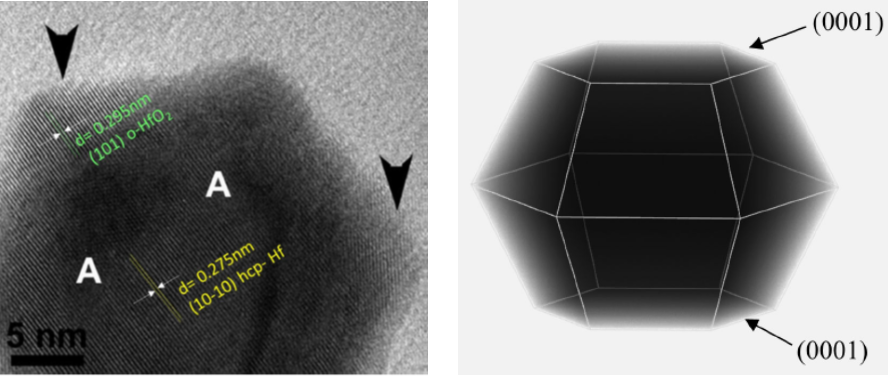
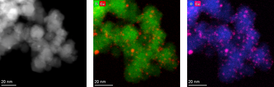
We develop and apply a variety of transmission electron microscopy techniques in order to study materials and nanostructures including conventional and high resolution transmission & scanning/transmission electron microscopy (HR-TEM, HR-S/TEM), energy dispersive X ray spectroscopy (EDS), electron energy loss spectroscopy (EELS) and energy filtered transmission electron microscopy (EFTEM). These methods are used to study the morphology, crystal structure and defects, chemical composition, valency and chemical bonding of a wide range of materials, nanostructures, thin films and interfaces such as oxides, alloys, ceramics, semiconducting, magnetic, composite and 2-D materials for various applications in energy, environment, health care, construction and information & communication technology. In order to fulfill the requirements emerging from the study of so diverse types of materials, specific protocols and methods are developed and applied. The experimental analysis is augmented by visualization-quantification-simulation procedures utilizing dedicated and in-house developed software.