Zinc oxide nanostructures
ZnO is a wide band gap (3.3 eV) semiconductor, which has been the subject of intense interest in recent years. The attractive features of ZnO for optoelectronic applications, in addition to its wide band gap are its high exciton binding energy (60 meV) and the high electron mobility. These -among others- properties are the reason that ZnO is envisaged for a variety of applications concerning solar cells, photocatalytic cells, sensors, memristors and optoelectronics to mention but a few.
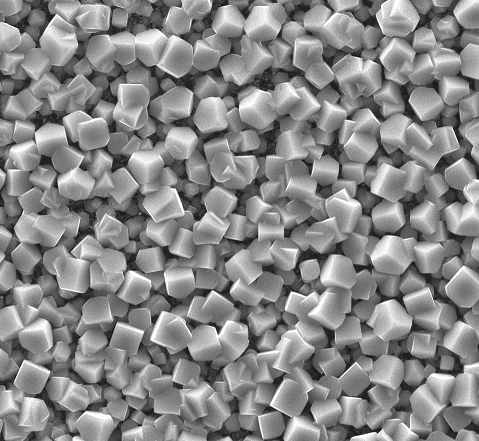
We fabricate a variety of ZnO nanostructures, such as nanorods, nanowires, nanoparticles, thin films, employing chemical and electrochemical methods we developed on a wide range of substrates. We tailor the morphology and dimensions of the ZnO nanostructures by varying the growth conditions.
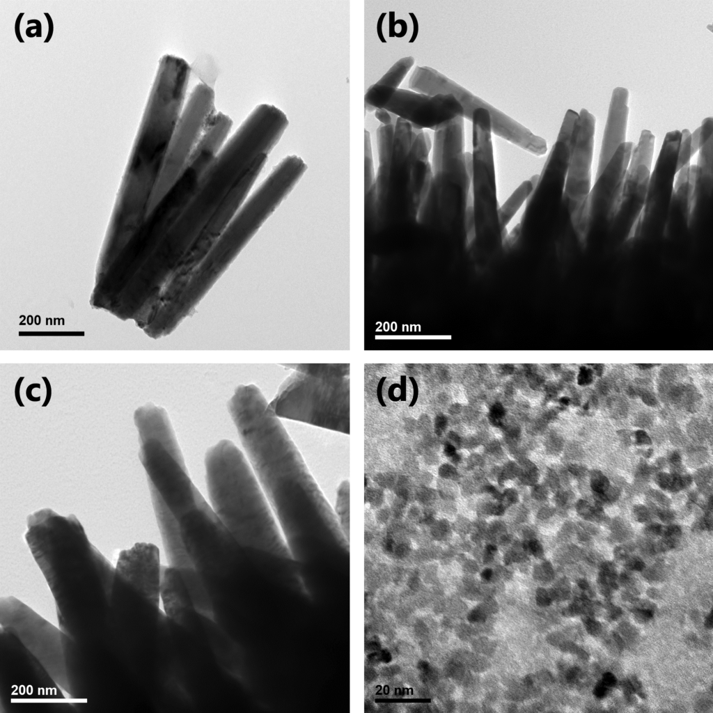
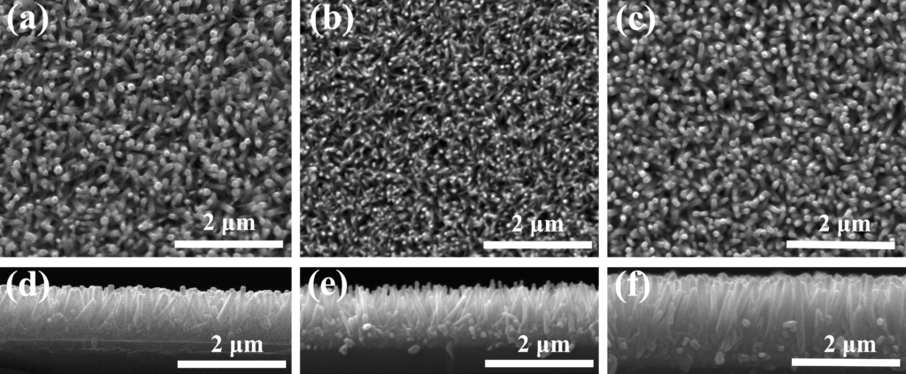
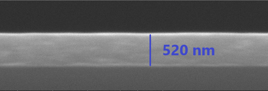
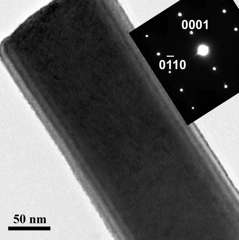
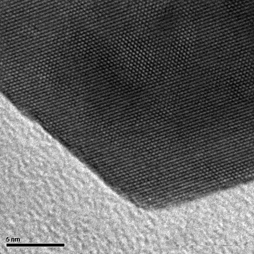
We use Scanning Electron Microscopy and Transmission Electron Microscopy techniques in order to study the morphology and crystal structure of the ZnO-based nanostructures and relate the growth conditions with their shape, size, crystal structure and defects as well as chemical composition.
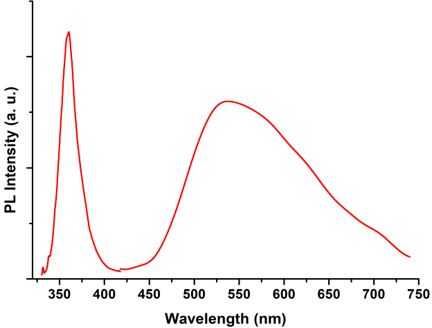
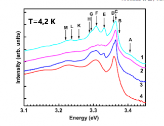
The intrinsic point defects, such as zinc and oxygen vacancies, interstitials and antisites, which play a profound role in the electrical behavior of ZnO, have extensively been studied in ZnO nanostructures specifically grown with large concentrations of such defects with photoluminescence spectroscopy.
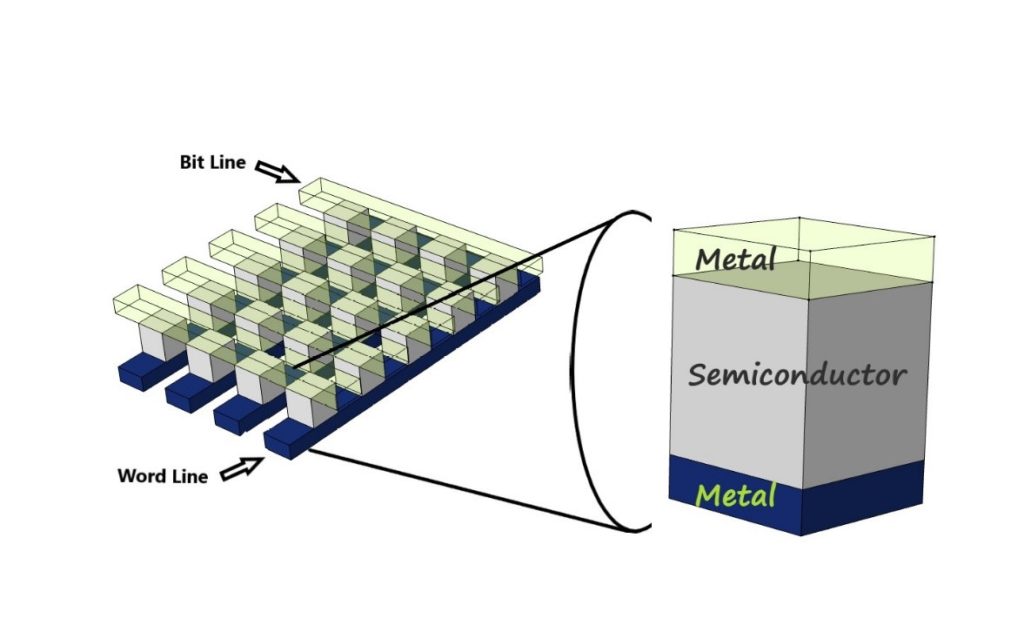
We use the functionalized ZnO nanostructures for a variety of applications such as heterostructure p-n junctions and memristors.