AI-Enhanced Computational Nanometrology
In this activity, we focus on the development of mathematical and computational methods including machine learning techniques for the metrological characterization of nanostructure morphologies. The motivation is emanated from the extreme requirements of accuracy on nanoscale which cannot be covered by advances in microscopy hardware only and the increased complexity of nanomorphologies which demands for advanced methods of quantitative characterization. Since plasma technology is used in both well-defined nanopatterns and open (freeform) surfaces, this activity can be separated in two parts:
A. Nanometrology of patterned structures
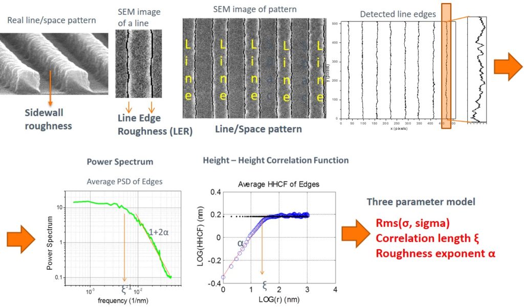
Line Edge Roughness (LER) concerns the sidewall roughness of line/space patterns and is of primary importance in current sub-20nm semiconductor research and industry. During the last two decades, we have pioneered the metrology of LER with the development and application of novel mathematical and computational tools focusing on the spatial and scaling/frequency analysis of LER (including Height-Height Correlation Function (HHCF), Power Spectral Density (PSD), (multi)fractal analysis and the related parameters of the correlation length, roughness exponent and fractal dimension i.e. the widely accepted and used three-parameter model for LER characterization proposed by our group). Finally, we are a member of the initiative of SEMI standards for the redefinition of the protocol for LER measurement. Our research targets:
A.1 Accuracy issues, such as noise removal from Scanning Electron Microscope (SEM) images
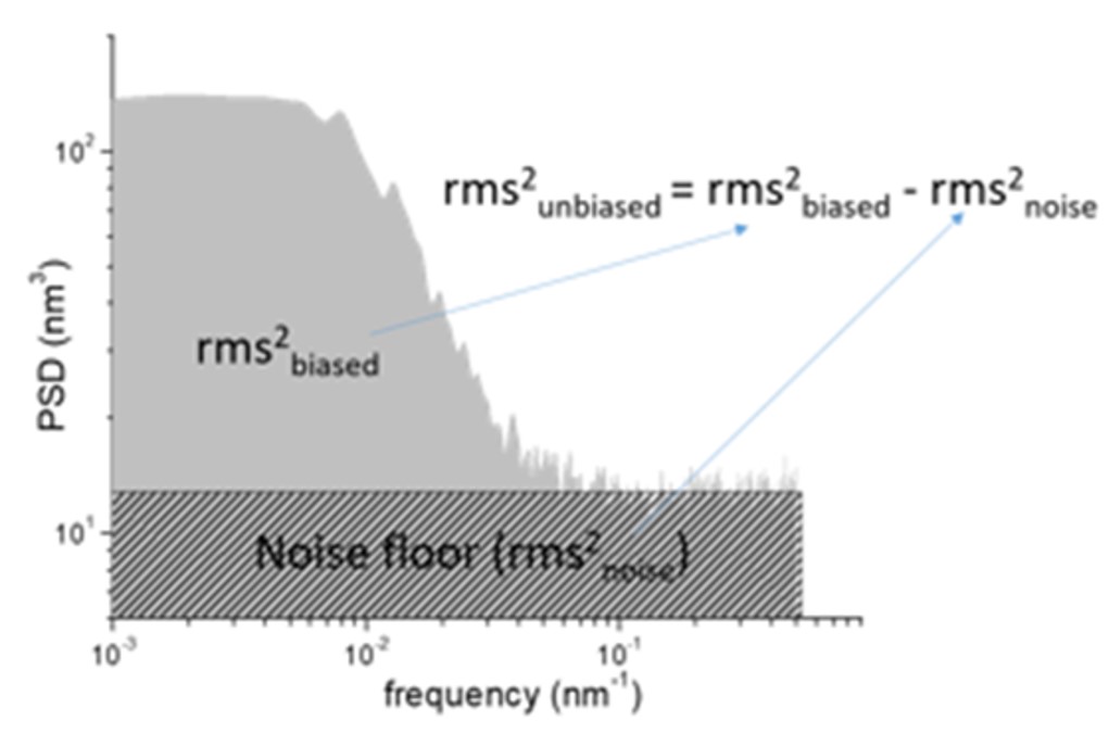
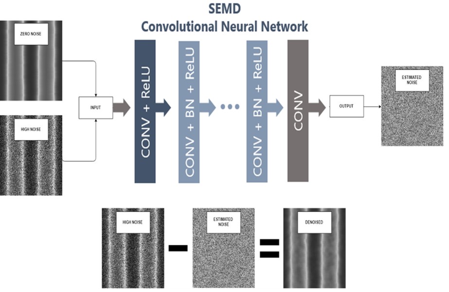
LER is usually measured through the analysis of top-down Scanning Electron Microscope images. However, they suffer from the presence of noise which degrade the accuracy of LER measurements on nanoscale. In order to mitigate noise effects and control their impact, we have developed two strategies.
- Fourier analysis (Power Spectral Density, PSD) to decompose image noise contribution to LER and acquire unbiased results (see Fig.1) and
- machine/deep learning techniques for the identification of noise effects on the whole image (convolutional neural network) or the edge profile (Hidden Markov Models) and the consequent denoising of images (see Fig.2)
Additionally, we developed a computational modeling to generate computer synthesized grayscale images with controlled levels of noise and LER characteristics. These computer synthesized images imitate closely the real SEM images and are used for validation of PSD-based method and the training of the convolutional neural network and other machine learning models. (see Fig.3). Finally, we have focused on the pixelization effects of SEM images on LER measurement and proposed an approach based on mathematical analysis to remedy these effects and obtain the true LER values.
A.2 Completeness issues such as cross-line correlations, and placement errors
Recently, new challenges in LER metrology have emerged by advances in nanopatterning techniques. In order to address these:
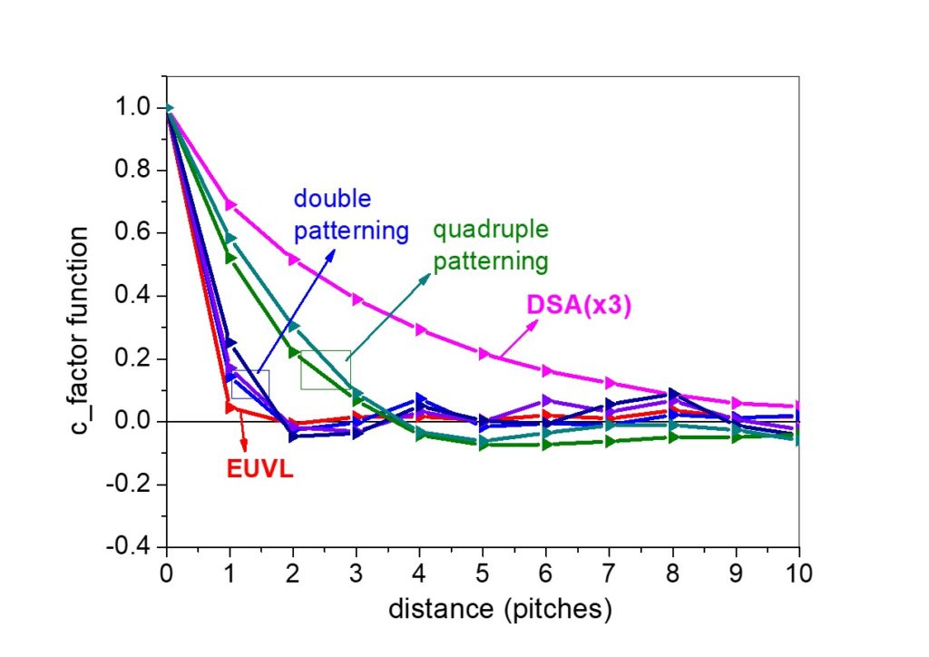
- We developed a novel methodology (c-factor correlation function and length) to capture the cross-line correlations critical in patterns with high densities (small pitch) and those produced by Directed Self-Assembly and Multi-Patterning lithographies. (see Fig.4)
- We initiated a hierarchical approach for the mathematical characterization of a real pattern targeting the identification of the two scales (pitch and CD) defining the line patterns and the two directions (across and along line direction) that correlations and deviations can appear.
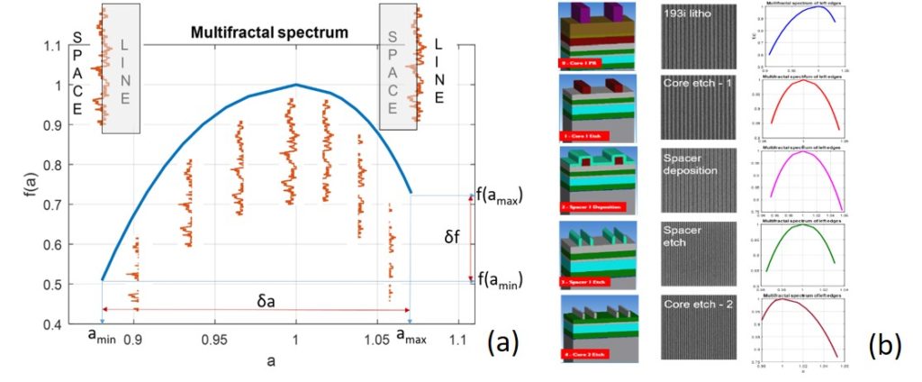
- We applied the multifractal analysis properly adapted in LER characterization. (see Fig.5)
We work on Edge and Pattern Placement Error and its relation with LER, targeting design rules of modern circuits taking LER into account.
B. Nanometrology of open (freeform) complex surfaces
Plasma processing and surface engineering in general produce surfaces with a rich variety and enhanced complexity of nanomorphologies. The aim of the second part of this activity is to cope with the challenge of the quantification and modeling of complexity and hierarchy in multiscale structures along with methods for the improvement of image quality (see the review paper: Kondi A, Papia E-M, Stai E and Constantoudis V (2025) “Computational methods in nanometrology: the challenges of resolution and stochasticity” Front. Nanotechnol. 7:1559523 doi: 10.3389/fnano.2025.1559523). To this end, we have developed and implemented methods based on
(a) Signal Analysis of Electron and Scanning Probe Microscopy (SM) Images - including Fourier and correlation analysis - enabling three key capabilities:
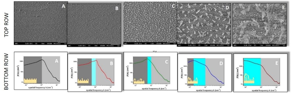
i) Identification, characterization and modeling of hierarchical surfaces with focus on the cross-scale interactions between hierarchical levels (see Fig.6) (G.Papavieros et.al., 2023 Nanotechnology 34 405702, DOI 10.1088/1361-6528/ace3c8)
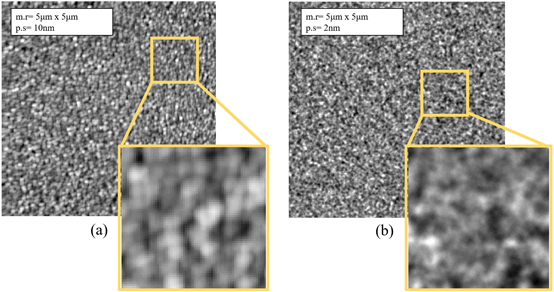
ii) Enhancement of image resolution in SM images using the generative Fourier Spectra Stitching (gFSS) method. gFSS method processes a small dataset of images captured at varying magnifications—via electron or scanning probe microscopy—and synthesizes new surfaces that are statistically similar with the input images. The resulting images of surface retain the large field of view of low-magnification image while having the high resolution (small pixel-size) of high-magnification image (see Fig.7) (Stai, E., Constantoudis, V., Kaidatzis, A., Singh, V., Tiwari, M. K., and Gogolides, E. (2025) “Generative resolution-enhanced microscopy based on computational stitching of Fourier spectra” 2025 Micron, 196-197 103867, DOI 10.1016/j.micron.2025.103867)
iii) Quantitative characterization of the verticality of nanowires developed on surfaces utilizing the anisotropy of the Fourier spectrum of both top-down and tilted SEM images of the surface to accurately determine whether nanowires are aligned and oriented vertically to the substrate (NWV method).
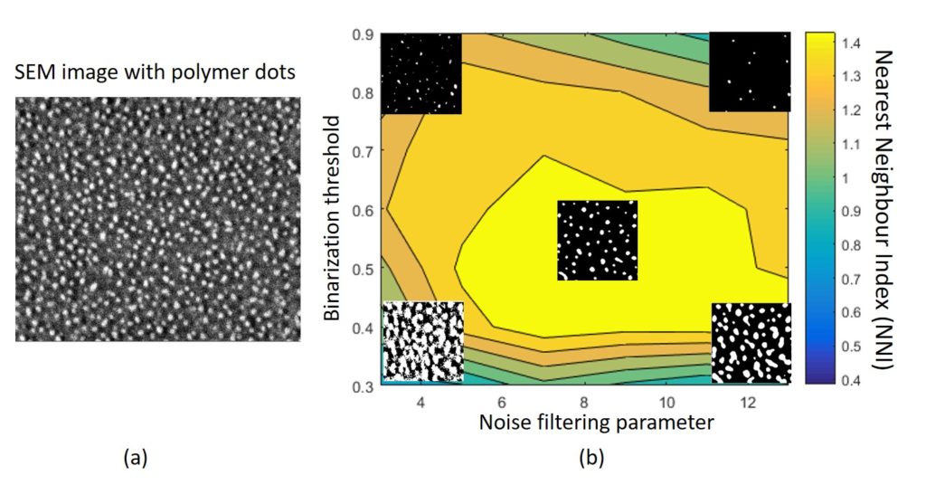
(b) Stochastic geometry (Point Pattern analysis), for the quantification of the extent of order/randomness of the positions of distinct nanostructures (nanoparticles, nanodots, nanowires) on a substrate. Also, the impact of image processing steps (denoising, binarization) on stochastic geometry metrics in real SEM images has been investigated (see Fig.8) (Mavrogonatos, A., Papia, E.-M., Dimitrakellis, P., and Constantoudis, V. (2022) “Measuring the randomness of micro and nanostructure spatial distributions: effects of Scanning Electron Microscope image processing and analysis” J. Microsc. 289, 48–57, doi:10.1111/jmi.13149).
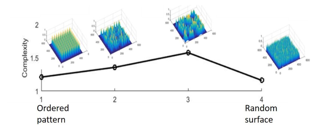
(c) Complexity science (multiscale entropies, chaos-based complexity and multifractality) for measuring the complexity of nanostructured surfaces using the concept of statistical/average symmetry. The concept of multiscale entropy is applied to quantify scale dependent surface heterogeneity, demonstrating that careful histogram binning eliminates amplitude driven distortions and isolates the intrinsic spatial complexity of nanoscale morphologies. As for the chaos-based complexity metric, the key idea is to use chaotic dynamics as a tool for the mixing of pixels of surface microscope images. The surface complexity can then be characterized by the “resistance” of surface morphology to this degradation process and quantified by the inverse of the decay rate of image information loss caused by the chaos-based mixing process. This idea has been implemented by using the Arnold cat map for the mixing and has been validated on synthetic self-affine and noisy images with controlled correlation length and roughness exponent. It has also applied to SEM images of aluminum surfaces etched in hydrochloric acid for different durations (Kondi, A., Constantoudis, V., Sarkiris, P., Ellinas, K., and Gogolides, E. (2023). Using chaotic dynamics to characterize the complexity of rough surfaces. Phys. Rev. E 107, 014206. doi:10.1103/PhysRevE.107.014206, Arapis, A., Constantoudis, V., Kontziampasis, D., Milionis, A., Lam, C. W. E., Tripathy, A., et al. (2022). Measuring the complexity of micro and nanostructured surfaces. Mater Today Proc. 54, 63–72. doi:10.1016/j.matpr.2021.10.120, Kondi, A.; Constantoudis, V.; Sarkiris, P.; Gogolides, E. Quantifying the Complexity of Rough Surfaces Using Multiscale Entropy: The Critical Role of Binning in Controlling Amplitude Effects. Mathematics 2025, 13, 2325, doi:10.3390/math13152325)
(d) The concept of spatial and structure symmetries. In particular, a symmetry-based analysis has been developed to characterize the deviation of nanostructure morphologies from perfect translational and scaling symmetries (see Fig.9) (V. Constantoudis, I. Ioannou-Sougleridis, A. Dimou, A. Ninou, M. Chatzichristidi, E. Makarona, “A symmetry-based approach to the characterization of complex surface morphologies: Application in CuO and NiO nanostructures”, Micro and Nano Engineering, 16, 2022, 100148, doi:10.1016/j.mne.2022.100148).
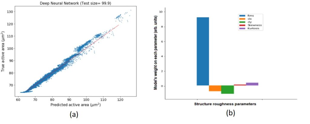
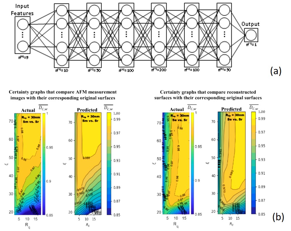
(e) Machine learning (neural networks, random forests) in order to link surface morphology to surface functionality (see Fig.10). Artificial neural networks have also been used to evaluate the importance of tip effects in the accuracy of surface roughness measurement with Atomic Force Microscope (see Fig.11). (Papia, E.-M., Kondi, A., and Constantoudis, V. (2024b). “Inverse design of hexagonal moiré materials: machine learning for tunable pore properties,” in Proceedings of the 13th hellenic conference on artificial intelligence (New York, NY, USA: Association for Computing Machinery). doi:10.1145/3688671.3688744, Kondi, A., Papia, E.-M., and Constantoudis, V. (2024). “Machine learning applications in nanotechnology manufacturing: from etching accuracy to deposition prediction,” in Proceedings of the 13th hellenic conference on artificial intelligence (New York, NY, USA: Association for Computing Machinery), doi:10.1145/3688671.3688740, Efi-Maria Papia, Alex Kondi, Vassilios Constantoudis, Machine learning applications in SEM-based pore analysis: a review, Microporous and Mesoporous Materials, Volume 394, 2025, 113675, doi:10.1016/j.micromeso.2025.113675)
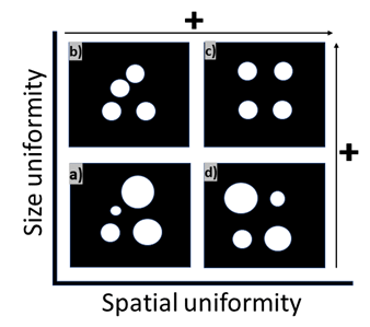
C. Nanometrology of fibrous and porous materials
The nanometrology of fibrous and porous materials integrates characterization methods to quantify both size uniformity and spatial uniformity at the nanometer scale (see Fig. 12). Central to this approach is the evaluation of spatial point patterns that characterize the arrangement of pore centroids or fiber junctions within these materials. An analysis tool we employed is the Nearest Neighbour Index (NNI), which allows for precise measurement of the spatial distribution of points (e.g., pores or intersections of fibers). This method provides valuable insight into the aggregation or periodicity of these patterns, revealing essential structural traits that influence material performance. The work lays the foundation for developing tailored porous materials in fields such as membrane filtration, where controlling both size and spatial distribution is key to achieving desired functional properties. (Papia, E.-M., Constantoudis, V., Ioannou, D., Zeniou, A., Hou, Y., Shah, P., et al. (2024a). Quantifying pore spatial uniformity: application on membranes before and after plasma etching. Micro Nano Eng. 24, 100278. doi:10.1016/j.mne.2024.100278, Efi-Maria Papia, Alex Kondi, Vassilios Constantoudis, Machine learning applications in SEM-based pore analysis: a review, Microporous and Mesoporous Materials, Volume 394, 2025, 113675, doi: /10.1016/j.micromeso.2025.113675).