Plasma Nanotechnology and Group History
Plasma is considered as the fourth state of matter and consists of a partially ionized gas containing neutral radicals, positive and often negative ions, and electrons. The plasma is quasi neutral. Typically, plasmas used for materials processing and nanotechnology are of relatively low electron density (i.e. number of electrons is less than one millionth of the gas molecules), and are “cold”, meaning that the gas is at a relatively low temperature of 300-500 K, electrons are “hot” with temperature larger than 11600 K (1eV). These hot electrons are responsible for gas ionization, dissociation to useful radicals, and photon emission. Plasmas in vacuum have been extensively used for nanoelectronics fabrication for film deposition, film etching, patterned film etching for nanostructure fabrication, ion implantation and various other processes. The 80s, and 90s are the times when a first revolution in plasma technology has taken place due to the amazing speed of the micro and nanoelectronics industry. Today, we are at the age of “nanoplasma” being able to etch down nanoscale features through nanoscale lithographically defined patterns. Examples are silicon nanopillars created by plasma etching after electron beam lithography.
Plasmas are also ideal for engineering the surface of materials, especially temperature sensitive ones, and changing the surface properties creating smart multifunctional material surfaces. Examples are superhydrophobic and superoleophobic surfaces repelling water and oils, fabricated by plasma processing.
Plasmas are also ideal for maskless nanostructure fabrication on metals, as well as nanomaterial fabrication. During the past decade plasma nanoscience and plasma nanotechnology has emerged as a second revolution in plasma technology (see special issue: Perspectives in Plasma Nanoscience edited by K. Ostrikov et al ).
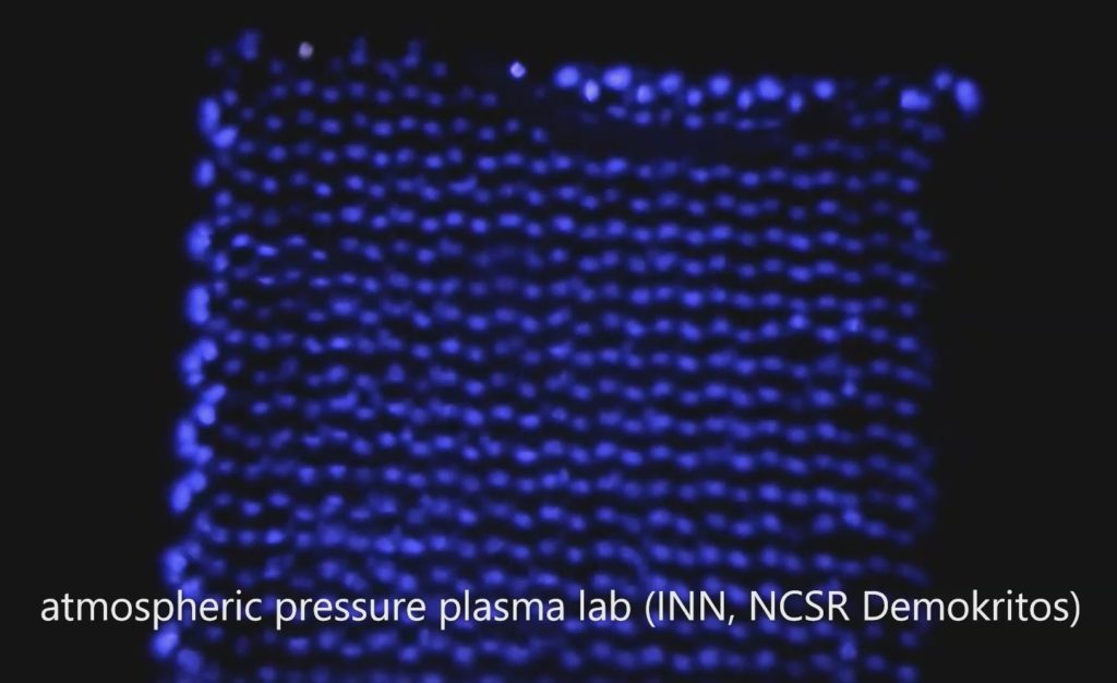
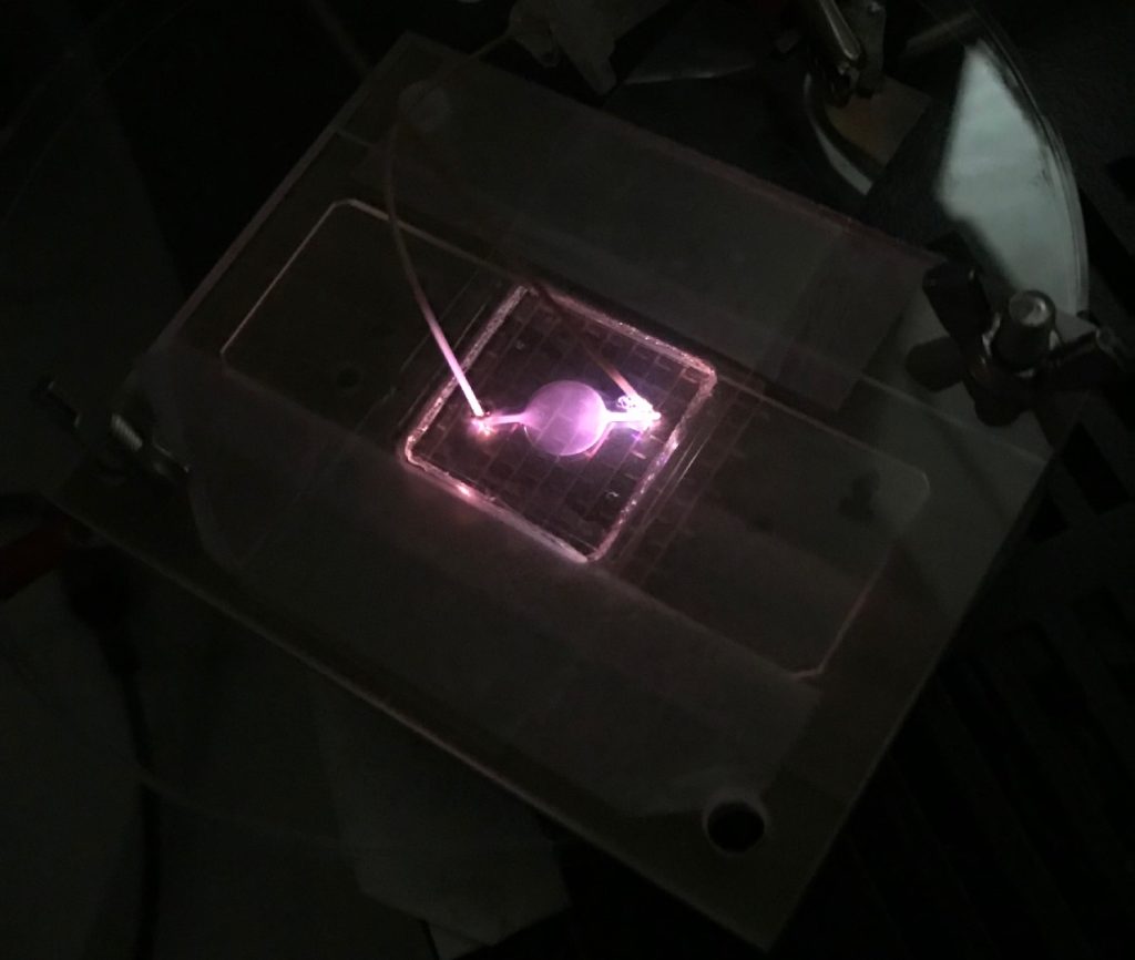
In the last few years we are witnessing the third revolution in plasma technology, by moving away from vacuum processing to atmospheric pressure plasma processing of materials for medicine, agriculture, safety, and of course surface engineering of large surfaces. We have invented both, wafer scale atmospheric pressure Dielectric Barrier Discharge apparatus, and smaller ones tailored to the size of a particular microfluidic device. See also relevant publications from our group in nanopattern formation with atmospheric plasma, a review of wetting control via atmospheric plasmas and a microfluidic device for bone marrow-on-a-chip.
Evolution of our research activities through the years
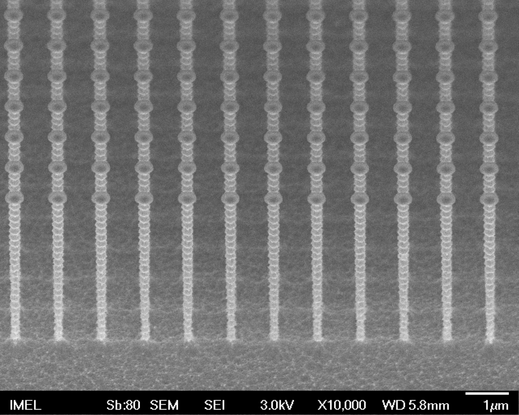
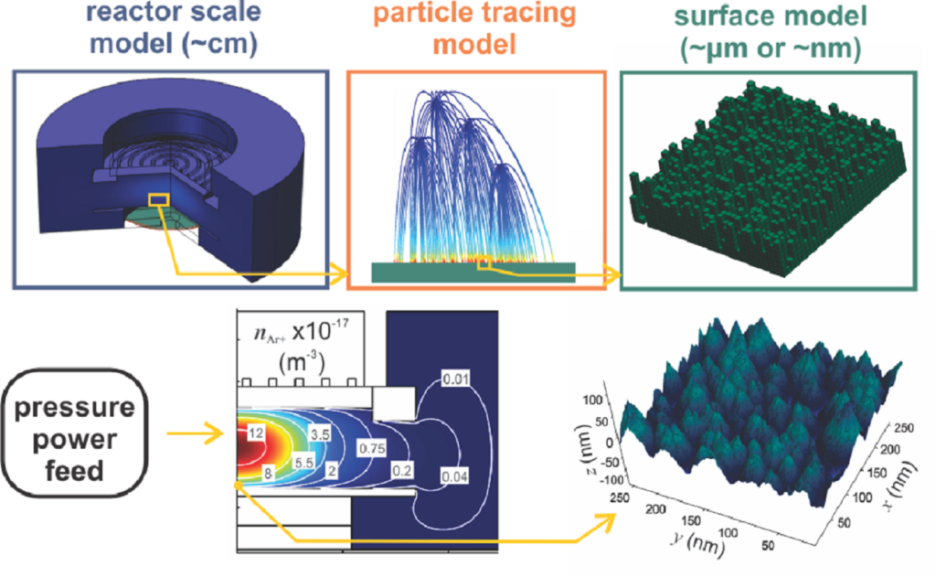
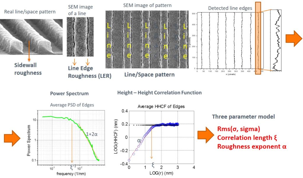
We have been following and pioneering as a group the evolution of plasma technology and processing. Starting from plasma etching of polymers and Silicon, plasma etching simulation, nanometrological analysis of line edge roughness patterns after lithography and plasma etching we have moved to nanoscale silicon etching for ultra-high aspect ratio silicon nanopillars.
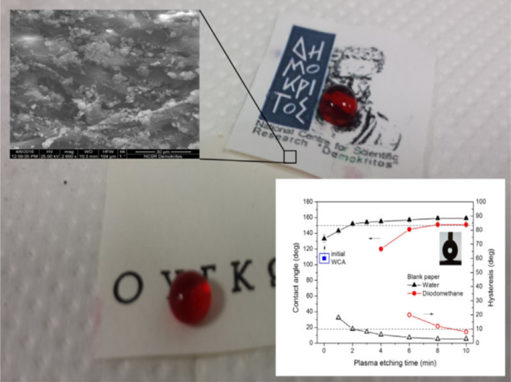
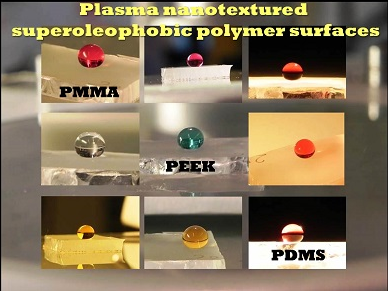
Then we pioneered a revolutionary plasma technology, which we term plasma micro-nanotexturing for polymeric surfaces, and have created multifunctional polymers with superhydrophobicity, superhydrophilicity, superamphiphobicity, optical property control, biomolecule adhesion control, cell growth control, and antibacterial properties. In addition, we applied such modifications in microfluidics creating “smart” functional microfluidics. Our efforts are reviewed in a recent publication. The work in microfluidics and Lab on Chip has increased significantly and a related new group was started within INN. Recently, we showcased atmospheric Dielectric Barrier Discharges for etching and wetting modification of polymers, fabricating superhydrophobic paper, and demonstrating etching and nanofabrication for the first time using atmospheric pressure plasma. Our work in vacuum and atmospheric pressure plasmas is expanding rapidly in new fields, such as food preservation, new “smart” functionalities, such as antifogging surfaces, and recently Superhydrophobic membranes for waste treatment towards zero liquid discharge, desalination and other environmental applications.