Collaboration with the Clean Room Facility for Nanoelectronics and MEMS
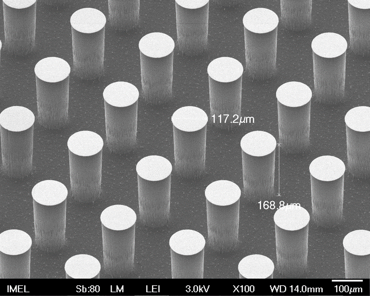
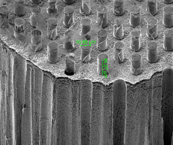
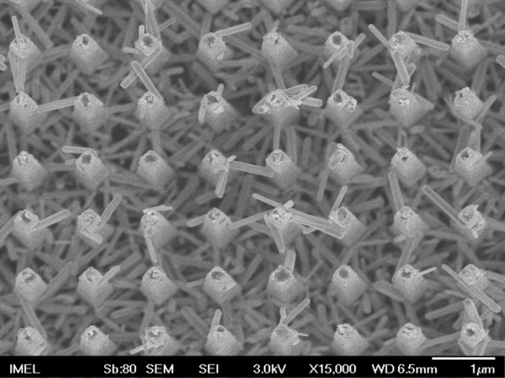
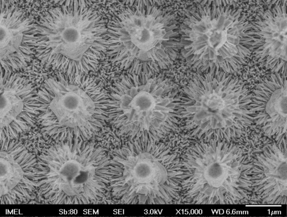
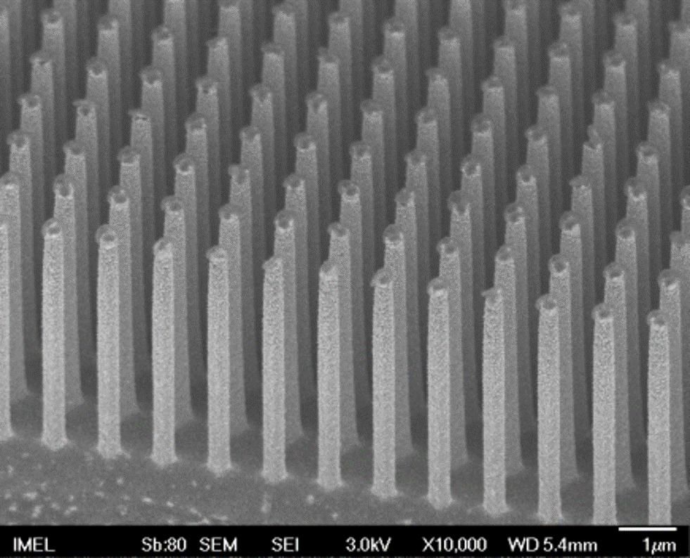
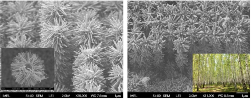
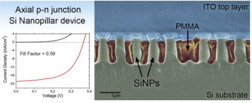
Working hand in hand with the clean room for Nanoelectronics and MEMS research and R&D services through the Innovation-ELWe work in close collaboration with the clean room facility of INN, often transferring samples between the clean room and the plasma laboratory and offering our expertise to colleagues who etch Si or Polymers for microsystems and sensors, and for any new material for which plasma processing research is needed. Examples include deep silicon etching of hierarchical structures for stamps, silicon nanopillar transistors with radial or axial junctions, Silicon nanopillars for triboelectrics, organic electronic device processing and many others. We also offer our expertise in plasma processing through the Innovation-el network (Innovation-el – Your Gateway to the Greek Infrastructure Network for Nanotechnology, Advanced Materials and Micro/Nanoelectronics).
The acquisition of the new etching tool [Atomic Layer Plasma Etching System (ALE)], stationed inside the clean-room facility, expanded the plasma groups’ capabilities over more advanced plasma etching techniques (atomic layer sequential etching, low-frequency, or pulsating plasma etching), of higher etching precision, pattern fidelity, and substrate variety. At the same time, an electron-beam evaporator (EBME) to deposit films of a variety of metals, with capabilities of co-deposition and alloy formation, as well as the first-in-Greece low-temperature thermal evaporation system (LTE-TSM & TEM) for sensitive and organic materials deposition, are two tools that were added to the general activities of the group. Members of the group are actively working to develop processes and novel techniques for the new tools inside the clean-room.