Atmospheric Pressure Plasma Technology
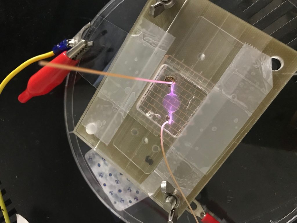
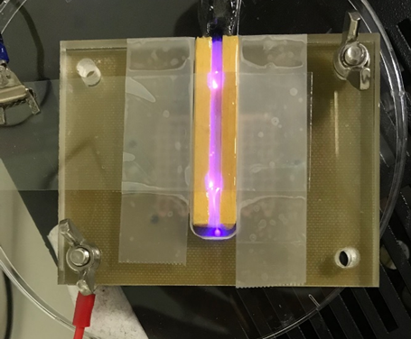
We have been working for several years on dielectric barrier discharges (DBD) for larger area surface processing and nanofabrication. A novel patented DBD design has allowed us to process large area samples, (see our recent EPO patent for large area atmospheric pressure device). Just as in vacuum plasmas our new device is based on selective shielding of the RF fields. This work in atmospheric plasmas has allowed us again to spin-out several applications towards surface engineering, food processing, and “smart” functional surfaces. In addition, we have observed surface nanostructure formation with atmospheric plasma, and etching and nanofabrication for the first time using atmospheric pressure plasma. A review article has also been published on our work on atmospheric pressure plasmas for material hydrophobization.
Atmospheric pressure plasma etching of nano-composite materials comprising components with different etching rates, has been used to reveal the content and morphology of the nanoscale phase.
In addition, atmospheric pressure plasma has been used to modify the internal walls of sealed microfluidic devices. The device can also be used as a surface discharge, allowing processing inside a container for example for food preservation, a topic discussed as a separate activity.
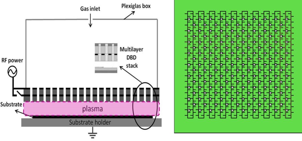
Large Area, Uniform, Atmospheric Pressure Plasma Processing Device
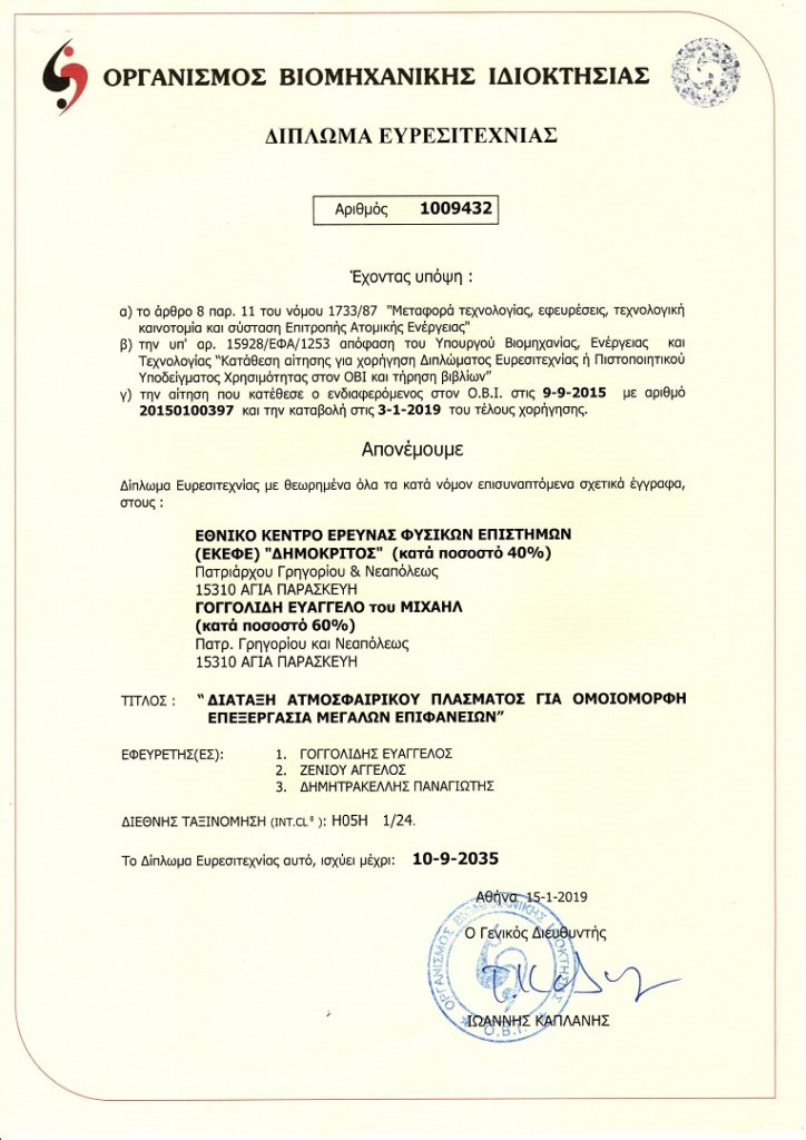
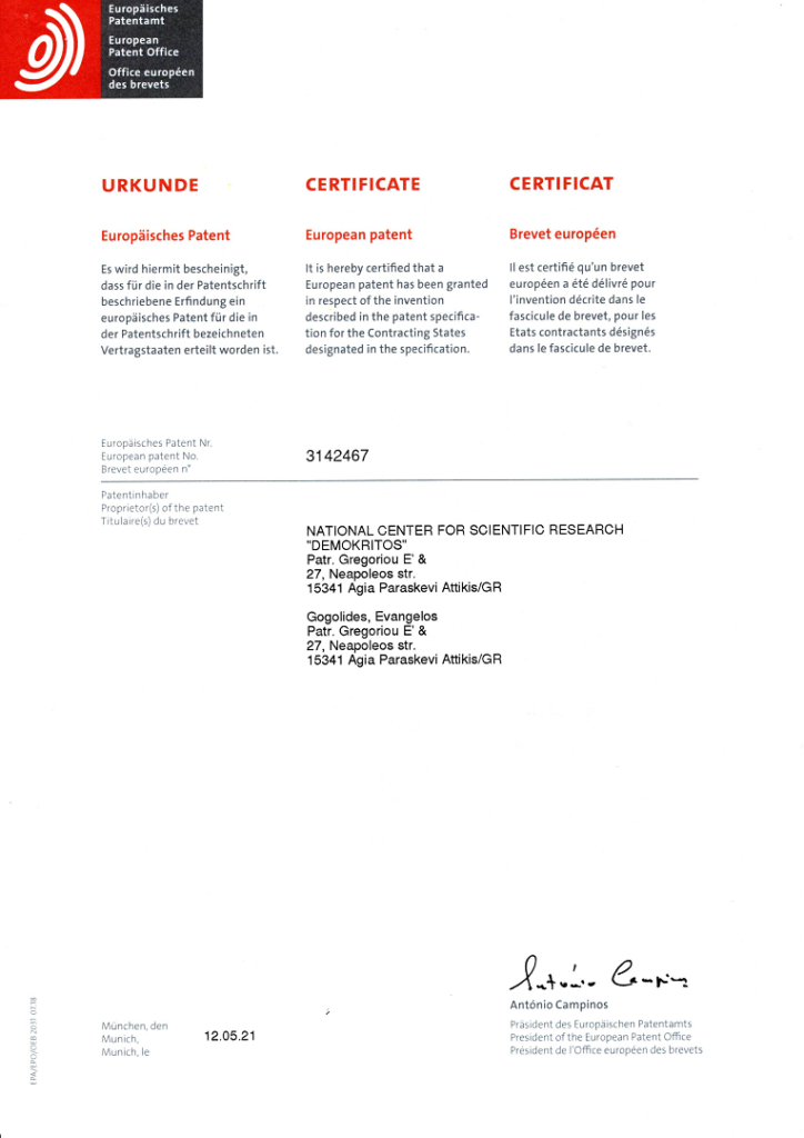
Greek patent application 20150100397 – 09/09/2015, Patent grant No. 1009432European patent application 16386016.6 – 08/09/2016, Patent grant No. EP3142467, 2021