Vacuum Plasma Technology and Nanofabrication
A. Plasma Etching for Nanofabrication
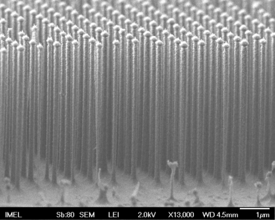
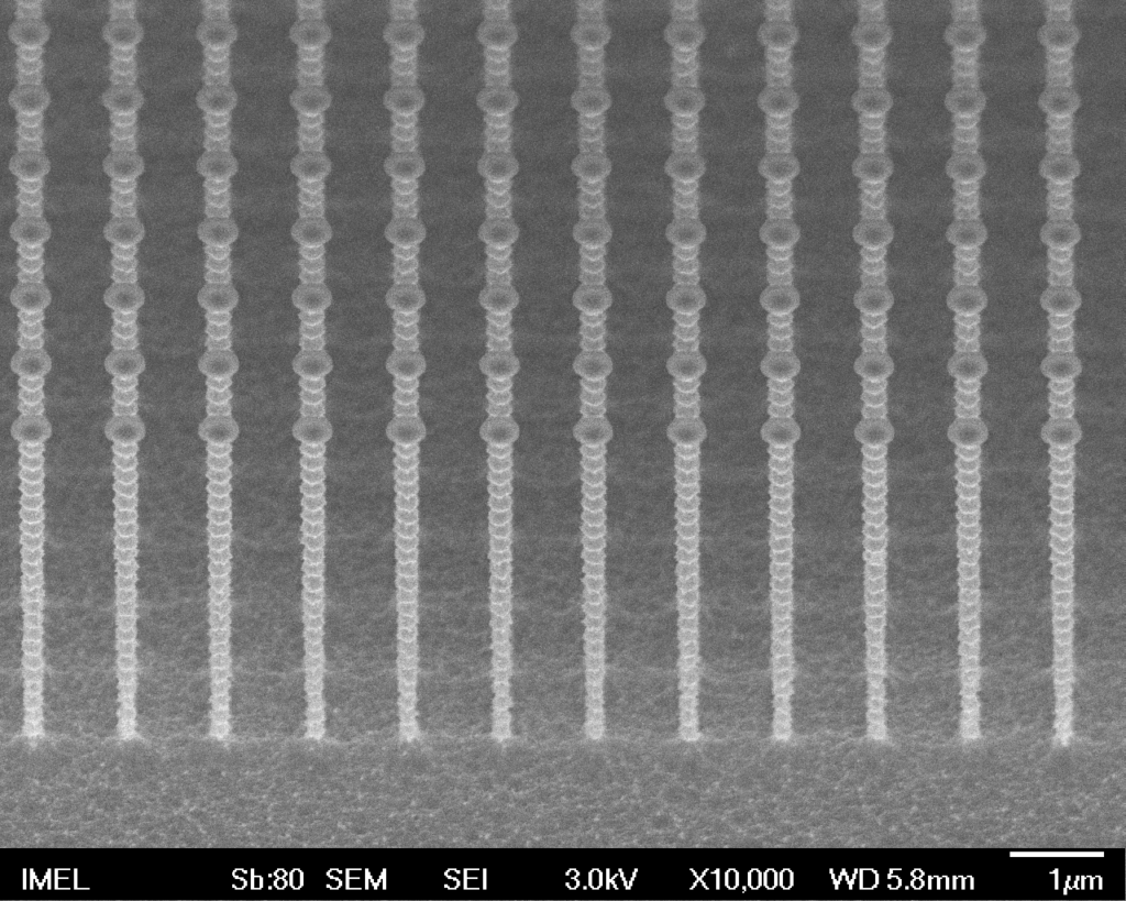
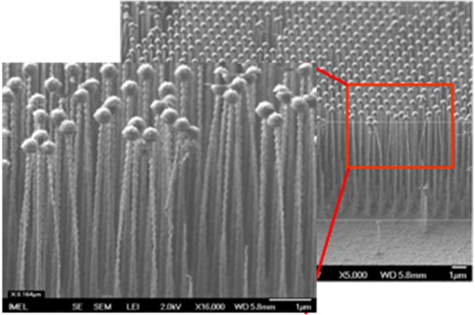
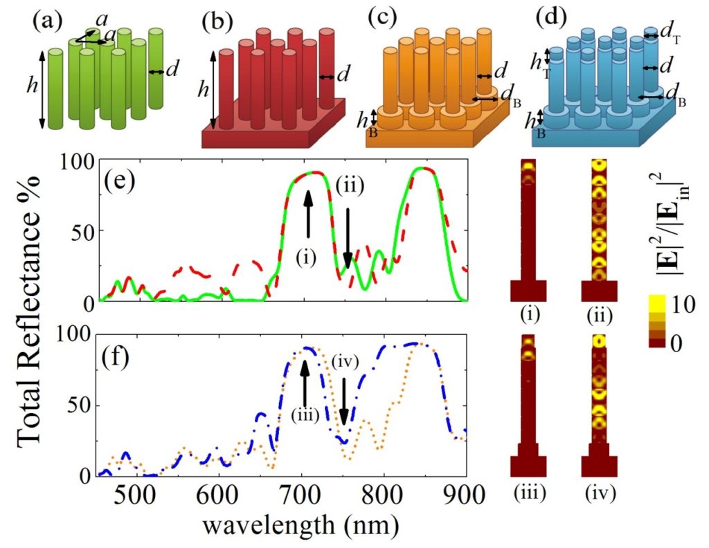
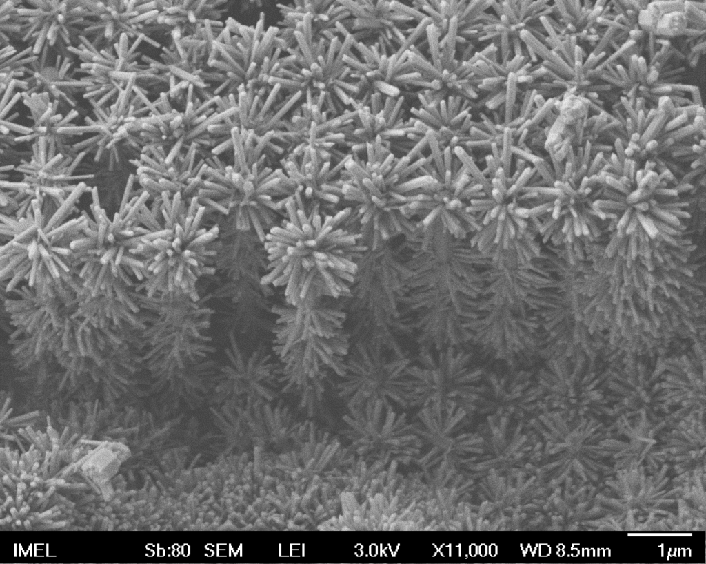
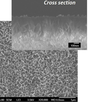
We have been active in nanoscale etching of Silicon creating ultrahigh aspect ratio silicon nanowires perpendicular to the Silicon substrate using both cryogenic and nanoscale gas chopping (Bosch-like) processes. We have studied the bundling of these nanowires, their optical properties, and their application for radial or axial junction photovoltaic devices. In addition, growth of ZnO nanostructures on such nanowires was achieved towards 3D ZnO networks.
B. Plasma micro-nanotexturing
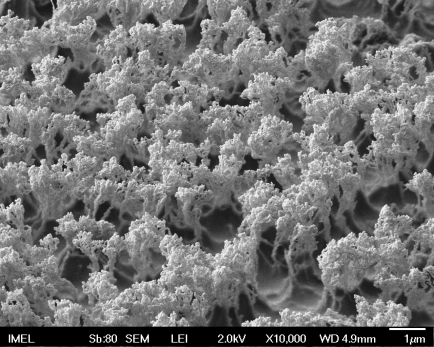
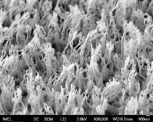
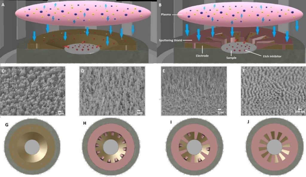
We have pioneered the plasma micro-nanotexturing technology and have designed and patented a novel related plasma reactor, which we term “nanoinhibit” reactor based on anisotropic ion-enhanced plasma etching with simultaneous controlled flux of co-sputtered etching inhibitors. The new plasma reactor is based on control of the area of electrode surface which is sputtered by ions. The control is achieved by a variable shield of specific areas of the electrode. This technology has allowed us to spin-out tens of different applications towards smart functional surfaces and devices. We have obtained an EPO patent on how to control the amount of texture produced during etching by changing the shielding of the biased electrode and the control in texture achieved by changing the amount of shielding.
C. Atomic Layer Etching (ALE)
Our group has been responsible for a large Infrastructure Project from HFRI (ELIDEK) entitled PlasmaForNano, for new plasma etching and material evaporation tools, which were installed in the clean room facility of the Institute. We acquired and installed these new micro/nanotechnology tools to develop novel processes, devices and micro/nano systems within the Greek research ecosystem. The plasma etching tool is an Atomic Layer (Plasma) Etching System (ALE) (available modes ALE, ICP, RIE), which is an advanced etch technique that allows for excellent depth control on shallow features. As device feature size reduces further and further ALE is necessary to achieve the accuracy required for peak performance. High fidelity pattern transfer (etching) is essential for the fabrication of todays advanced microelectronics devices.The second tool is an Electron Beam (E-beam) Metal Evaporator (EBME), which is a well-established physical vapor deposition technique for producing high-purity uniform metal coatings on solid or flexible substrates at a rate typically in the range of 0.1nm to 1μm/min. Lastly, a Low Temperature Evaporator for Temperature Sensitive Materials and Thermal Evaporator for Metals (LTE-TSM & TEM) was acquired, used in deposition by heating source materials to a relatively low temperature to produce vapor for thin-film coating processes, typically under vacuum conditions. The use of low temperature minimizes thermal damage to both the source material and the substrate, making it suitable for depositing heat-sensitive compounds such as organic materials and polymers.
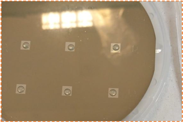
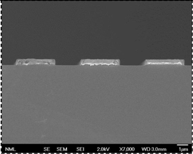
In the next figures results from preliminary demonstration projects, with the use of the above tools, are portrayed: a) a SERS substrate on Al coated silicon after boiling in water and coating with Silver, b) a nano-bio system demonstrator comprising of microwells containing SERS substrates and filled with drops of uric acid before analysis, and c) nano-electronic demonstrator showing interdigitated Al electrodes (Al was coated with the EBME, and after optical lithography was etched with the new ALPES).
D. Plasma directed formation of periodic nanoripples on polymeric substrates
We have studied quasi-periodic nanoripples formation on perpendicularly placed polymeric substrates with respect to the plasma reactor electrode near the bottom edge of the substrates (i.e. adjacent to the electrode). The plasma texturing of these perpendicular polymeric samples is rapid, easy and promising for fabricating in one-step (masklessly and without using intricate sheath control plates) quasi-periodic patterns. The term Plasma-Induced Periodic Surface Structures (PIPSS) for such periodic nanostructures is introduced - in correspondence with the well-established term Laser-Induced Periodic Surface Structures (LIPSS). Such nanoripples have become more and more attractive due to their capability to change the materials’ surface properties and can be utilized in a variety of applications from light harvesting to bioanalysis and microfluidics. This formation is attributed to ion trajectories reaching the substrate bottom edge with high off-normal angles, as predicted by a modeling framework calculating ion trajectories. More particularly a modelling framework comprising of a reactor scale model and a Monte Carlo particle tracing model is employed to predict the formation of anisotropic (quasi-periodic) structures (nanoripples) on the perpendicularly placed polymeric substrates through calculation of the local distributions of the ion incident angles and energies (IAEDF). The ions seem to “scratch” the polymeric surface leading to ripple formation, parallel to the ion direction, while when moving upwards, the ion impinging angle decreases, leading to a more isotropic roughened pattern. This variation from anisotropic (nanoripples) to isotropic pattern (nanowire-like) roughness was experimentally confirmed through plasma processing experiments on commercial polymeric samples, via SEM images and their metrological analysis.
Selected publications
- Athina S. Kastania, Sotiris Mouchtouris, Eleni Stai, Angelos Zeniou, George Kokkoris, Vassilios Constantoudis, Pavlos Tsavalas, Konstantina Mergia, Evangelos Gogolides, Angeliki Tserepi, Plasma-Induced Maskless Formation of Quasi-Periodic Nanoripples on Polymeric Substrates, Advanced Engineering Materials, Volume 27, Issue 7, 2025, [doi]
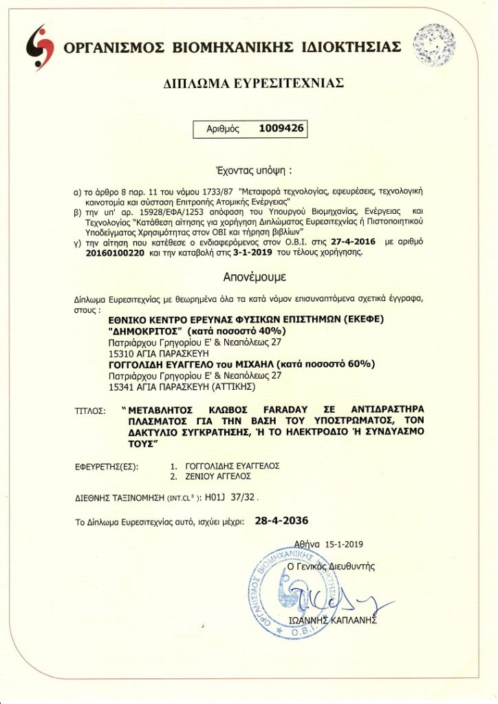
Variable Faraday shield for a substrate holder, a clamping ring, or an electrode, or their combination in a plasma reactor
Greek patent application 20160100220 – 27/04/2016, Patent grant No. 1009426
European Patent Granted in 2023