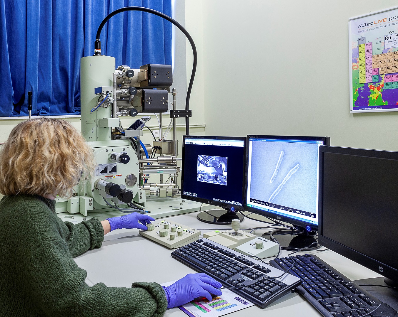
SEM Jeol JSM 7401F FE
SEM/EDS
Tool
JSM 7401F (JEOL) Field Emission SEM (FESEM) equipped with Xplore15 EDS (Oxford)
Applications
Conventional SEM operation. EDX nanoanalysis. General forensic investigation in the SEM. Gentle beam option to study non-conductive samples.
Materials: metals, ceramics and carbon, plastics, polymers, oxides, semiconductors, composites, nanoparticles, mixed oxides
Technical Specifications
Source: Cold field emission electron gun (Tungsten single crystal emitter)
Beam Voltage: 0.1 to 30 kV
Resolution: 1.0nm (15kV), 1.5nm (1kV)
Detectors: Three Electron Detectors + Camera: Upper secondary electron in-lens (SEI), Lower secondary electron (LEI), Retractable backscattered electrons detectors (RBEI) & IR camera
Stage: Eucentric goniometer stage.
Computer controlled 3-axis: X-Y: 70 x 50mm, rotation R:360o and manual handling of Z-axis: 1.5 up to 25mm and tilt from -5o up to +70o
Other Capabilities: Magnification up to x1.000.000, Vacuum down to 10-8Pa, Sample Size: From 10mm x 10mm to 10cm x 10cm, Maximum Sample Height: 10mm
EDS
Detector area: 15mm2
Resolution: Guaranteed Mn Ka<129eV resolution
Max count rates: in excess of 1Mcps
Additional Tools
Images